78
2467S–AVR–07/09
ATmega128
Note: 1. XMM = 0 in ATmega103 compatibility mode.
Alternate Functions of
Port D
The Port D pins with alternate functions are shown in Table 36.
Note: 1. XCK1, TXD1, RXD1, SDA, and SCL not applicable in ATmega103 compatibility mode.
The alternate pin configuration is as follows:
• T2 – Port D, Bit 7
T2, Timer/Counter2 counter source.
• T1 – Port D, Bit 6
T1, Timer/Counter1 counter source.
• XCK1 – Port D, Bit 5
XCK1, USART1 External clock. The Data Direction Register (DDD4) controls whether the clock
is output (DDD4 set) or input (DDD4 cleared). The XCK1 pin is active only when the USART1
operates in Synchronous mode.
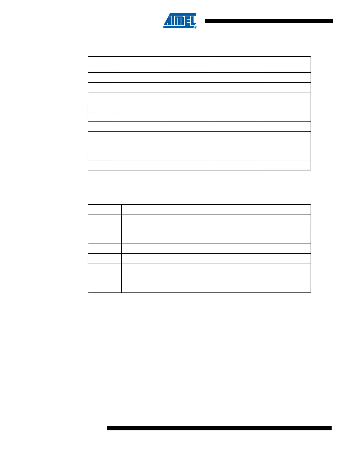
Table 35. Overriding Signals for Alternate Functions in PC3..PC0
(1)
Signal
Name PC3/A11 PC2/A10 PC1/A9 PC0/A8
PUOE SRE • (XMM<5) SRE • (XMM<6) SRE • (XMM<7) SRE • (XMM<7)
PUOV0000
DDOE SRE • (XMM<5) SRE • (XMM<6) SRE • (XMM<7) SRE • (XMM<7)
DDOV 1 1 1 1
PVOE SRE • (XMM<5) SRE • (XMM<6) SRE • (XMM<7) SRE • (XMM<7)
PVOV A11 A10 A9 A8
DIEOE0000
DIEOV0000
DI––––
AIO––––
Table 36. Port D Pins Alternate Functions
Port Pin Alternate Function
PD7 T2 (Timer/Counter2 Clock Input)
PD6 T1 (Timer/Counter1 Clock Input)
PD5 XCK1
(1)
(USART1 External Clock Input/Output)
PD4 ICP1 (Timer/Counter1 Input Capture Pin)
PD3 INT3/TXD1
(1)
(External Interrupt3 Input or UART1 Transmit Pin)
PD2 INT2/RXD1
(1)
(External Interrupt2 Input or UART1 Receive Pin)
PD1 INT1/SDA
(1)
(External Interrupt1 Input or TWI Serial DAta)
PD0 INT0/SCL
(1)
(External Interrupt0 Input or TWI Serial CLock)