INSTALLATION MANUAL
CMA-5024 GLSSU
This document includes Proprietary Information and shall not be reproduced or communicated to third party
without prior written permission by CMC Electronics Inc.
Page TC-5
November 21, 2008
LIST OF ILLUSTRATIONS
Figure Title Page
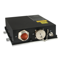
Figure 1. CMA-5024 GLSSU ....................................................................................................................3
Figure 2. Equipment Identification ............................................................................................................6
Figure 3. Typical Class Beta 3 dual GLSSU installation (one side shown)..............................................8
Figure 4. Typical Class Delta 4 dual GLSSU installation (one side shown).............................................9
Figure 5. Typical Class DELTA-4 dual GLSSU installation ......................................................................11
Figure 6. Typical retrofitted dual GLSSU ARINC743A-4 installation........................................................16
Figure 7. GLSSU Functional Block Diagram ............................................................................................18
Figure 8. Core Receiver Assembly Block Diagram ..................................................................................19
Figure 9. Applicable Standards (Sheet 1 of 2)..........................................................................................23
Figure 10. GLSSU Physical, Power and Reliability Specifications.............................................................25
Figure 11. GLSSU Environmental Specifications (Sheet 1 of 2) ................................................................26
Figure 12. GLSSU Performance Specifications (Sheet 1 of 2)...................................................................28
Figure 101. Typical Antenna Location ..........................................................................................................101
Figure 102. Typical GPS/SBAS antenna (for reference)..............................................................................104
Figure 103. Cable Loss Considerations........................................................................................................107
Figure 104. GLSSU Outline Drawing............................................................................................................109
Figure 105. GLSSU J1 connector (seen from the front of the GLSSU)........................................................110
Figure 106. Pin Assignments (Sheet 1 of 2).................................................................................................111
Figure 107. GLSSU approach aircraft connector J3 (seen from the front of the GLSSU) ...........................113
Figure 108. Pin Assignments for J3; ARINC-429 Data and Discrete Interfaces ..........................................114
Figure 109. Pin Assignments for J3; HIS Interfaces.....................................................................................115
Figure 110. Pin Assignments for J3; Future Analog/Digital Interfaces.........................................................116
Figure 111. Antenna Coaxial Connector Sleeving........................................................................................119
Figure A-1. SSM Bits Setting........................................................................................................................A.6
Figure A-2. ARINC 429 IRS/FMS Input Bus Data Labels ............................................................................A.9
Figure A-3. ARINC 429 FMS/DADS Input Bus Data Labels........................................................................A.10
Figure A-4. ARINC 419 DADS input bus data labels ...................................................................................A.10
Figure A-5. ARINC 429 X-Talk input bus data labels...................................................................................A.11
Figure A-6. ARINC 429 OMS input bus data labels.....................................................................................A.12
Figure A-7. ARINC 429 GP/DIFF input bus data labels...............................................................................A.12
Figure A-8. ARINC 429 Data Loader input bus data labels .........................................................................A.12
Figure A-9. ARINC 429 Freq/Function Data Source input bus data labels..................................................A.12
Figure A-10. ARINC 429 DME input bus data labels.....................................................................................A.13
Figure A-11. ARINC 429 ILS input bus data labels........................................................................................A.13
Figure A-12. ARINC Output Data (GPS bus) (Sheet 1 of 3)..........................................................................A.18
Figure A-13. ARINC Output Data (GLS bus) (Sheet 1 of 4) ..........................................................................A.21
Figure A-14. ARINC Output Data (ILS look-alike bus)...................................................................................A.25
Figure A-15. ARINC Output Data (DME look-alike bus) (Sheet 1 of 2) .........................................................A.25
LIST OF TABLES
Table Title Page
Table 1 Aircraft Personality Data - On/Off Options ................................................................................E.24
Table 2 Aircraft Personality Data - Numerical Parameters.....................................................................E.25
Table 3 Aircraft Personality Data - Label ID Assignments .....................................................................E.26
Table 4 Aircraft Personality Data – ILS/DME Look-Alike Options..........................................................E.27
Table 5 Aircraft Personality Data – Selectable ILS & DME ARINC 429 Labels.....................................E.28
Table G-1. Final Approach Segment Data Message Block format..............................................................G.1
The document reference is online, please check the correspondence between the online documentation and the printed version.
 Loading...