Copyright © 2014 congatec AG IGX1m02 119/134
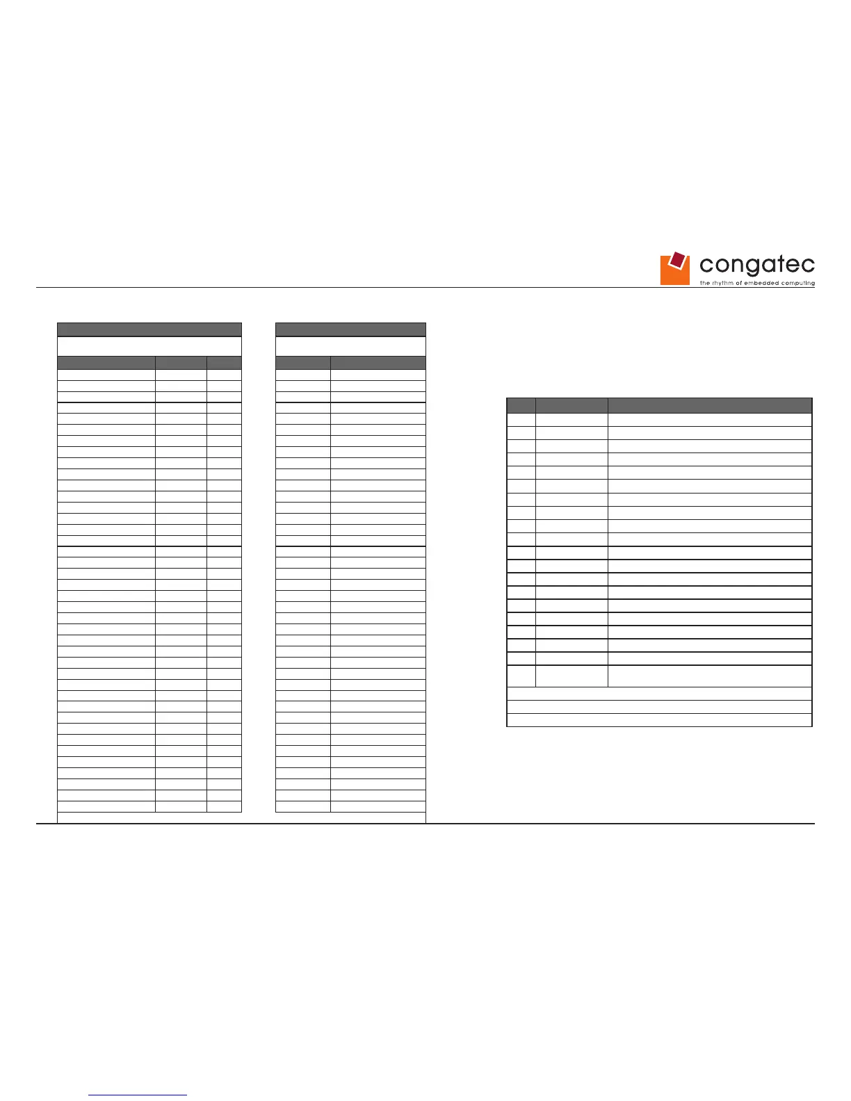
24.2 AUO_G150XG01 LVDS Cable Pinout
conga-IGX AUO-G150XG01
LVDS Connector Hirose DF13-40, straight, SMT
DF-14H-20P-1.25H (Hirose)
or CWY20G-A0D1T (PTWO)
Signal Symbol Pin Pin Symbol
Ground GND 1
Ground GND 2
◄▪▪▪▪▪►
20 GND
LVDS_Out3+ (ODD_3+) LO3+ 3
◄▪▪▪▪▪►
18 RxIN3+
LVDS_Out7+ (EVEN_3+) LO7+ 4
LVDS_Out3- (ODD_3-) LO3- 5
◄▪▪▪▪▪►
17 RxIN3-
LVDS_Out7- (EVEN_3-) LO7- 6
Ground GND 7
◄▪▪▪▪▪►
3 GND
Ground GND 8
◄▪▪▪▪▪►
4 GND
LVDS_Out2+ (ODD_2+) LO2+ 9
◄▪▪▪▪▪►
12 RxIN2+
LVDS_Out6+ (EVEN_2+) LO6+ 10
LVDS_Out2- (ODD_2-) LO2- 11
◄▪▪▪▪▪►
11 RxIN2-
LVDS_Out6- (EVEN_2-) LO6- 12
Ground GND 13
Ground GND 14
◄▪▪▪▪▪►
7 GND
LVDS_Out1+ (ODD_1+) LO1+ 15
◄▪▪▪▪▪►
9 RxIN1+
LVDS_Out5+ (EVEN_1+) LO5+ 16
LVDS_Out1- (ODD_1-) LO1- 17
◄▪▪▪▪▪►
8 RxIN1-
LVDS_Out5- (EVEN_1-) LO5- 18
Ground GND 19
Ground GND 20
◄▪▪▪▪▪►
10 GND
LVDS_Out0+ (ODD_0+) LO0+ 21
◄▪▪▪▪▪►
6 RxIN0+
LVDS_Out4+ (EVEN_0+) LO4+ 22
LVDS_Out0- (ODD_0-) LO0- 23
◄▪▪▪▪▪►
5 RxIN0-
LVDS_Out4- (EVEN_0-) LO4- 24
Ground GND 25
Ground GND 26
◄▪▪▪▪▪►
13 GND
LVDS_CLK1+ (CLK_ODD+) CLK1+ 27
◄▪▪▪▪▪►
15 CKIN+
LVDS_CLK2+ (CLK_EVEN+) CLK2+ 28
LVDS_CLK1- (CLK_ODD-) CLK1- 29
◄▪▪▪▪▪►
14 CKIN-
LVDS_CLK2- (CLK_EVEN-) CLK2- 30
Ground GND 31
◄▪▪▪▪▪►
16 GND
Ground GND 32
◄▪▪▪▪▪►
19 GND
DDC-Clock DDCCLK 33
DDC-Data DDCDATA 34
LCD-Power 1) +3.3V / +5V 35
◄▪▪▪▪▪►
1 VDD
LCD-Power 1) +3.3V / +5V 36
◄▪▪▪▪▪►
2 VDD
LCD-Power 1) +3.3V / +5V 37
Ground GND 38
Ground GND 39
LCD_PowerOn LCD_On 40
1) selectable via Jumper
Pin Signal Name Description
1 VDD Power Supply, 3.3V (typical)
2 VDD Power Supply, 3.3V (typical)
3 GND Ground
4 REV Reverse Scan [H: Enable; L/NC: Disable]*Note1,3
5 Rin0- - LVDS differential data input
6 Rin0+ + LVDS differential data input
7 GND Ground
8 Rin1- - LVDS differential data input
9 Rin1+ + LVDS differential data input
10 GND Ground
11 Rin2- - LVDS differential data input
12 Rin2+ + LVDS differential data input
13 GND Ground
14 ClkIN- - LVDS differential clock input
15 ClkIN+ + LVDS differential clock input
16 GND Ground
17 Rin3- - LVDS differential data input *Note2
18 Rin3+ - LVDS differential data input *Note2
19 NC/GND Reserved for AUO internal test. Please set it as NC or Ground.
20 SEL68
Selection for 6 bits/8bits LVDS data input[H/NC: 6bits, L:
8bits]*Note1,3
Note 1: Input signals shall be in low status when VDD is off.
Note 2: For 6bits input mode, pin 17 and pin 18 must be oated.
Note 3: High stands for “3.3V”, Low stands for “0V”, NC stands for “No Connection”.
24.2.1 Panel Pinout AUO G150XG01