Copyright © 2014 congatec AG IGX1m02 25/134
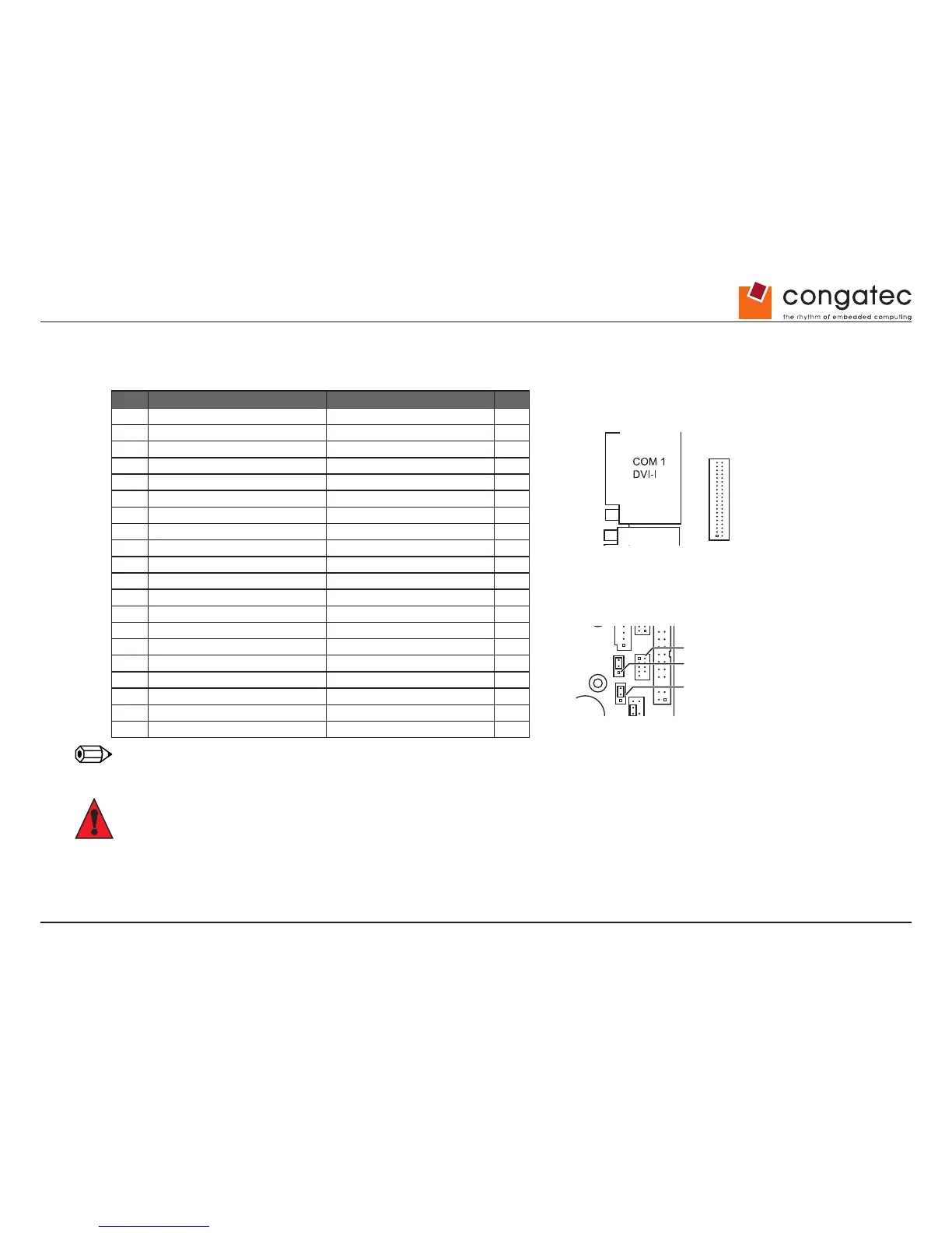
5.3 LVDS Connector details
LVDS Connector: Hirose DF13-40 (or compatible).
PIN SIGNAL SIGNAL PIN
2 Ground Ground 1
4 LVDS_H3+ (EVEN_3+) LVDS_L3+ (ODD_3+) 3
6 LVDS_H3- (EVEN_3-) LVDS_L3- (ODD_3-) 5
8 Ground Ground 7
10 LVDS_H2+ (EVEN_2+) LVDS_L2+ (ODD_2+) 9
12 LVDS_H2- (EVEN_2-) LVDS_L2- (ODD_2-) 11
14 Ground Ground 13
16 LVDS_H1+ (EVEN_1+) LVDS_L1+ (ODD_1+) 15
18 LVDS_H1- (EVEN_1-) LVDS_L1- (ODD_1-) 17
20 Ground Ground 19
22 LVDS_H0+ (EVEN_0+) LVDS_L0+ (ODD_0+) 21
24 LVDS_H0- (EVEN_0-) LVDS_L0- (ODD_0-) 23
26 Ground Ground 25
28 LVDS_CLK_H+ (CLK_EVEN_+) LVDS_CLK_L+ (CLK_ODD_+) 27
30 LVDS_CLK_H- (CLK_EVEN_-) LVDS_CLK_L- (CLK_ODD_-) 29
32 Ground Ground 31
34 DDC-Data DDC-Clock 33
36 LCD-Power (see note below) LCD-Power (see note below) 35
38 Ground LCD-Power (see note below) 37
40 LCD_Power_Enable Ground 39
Note
Selectable via jumper.
Caution
Maximum load: 1A per pin.
CPU
Memory Module 1
Memory Module 2
BIOS Recovery Settings
LVDS Supply Settings
USB 2.0
LVDS BL Control Settings
System Power On Settings
1
1
Fan 1 (CPU)
1 = GND
2 = 12 V PWM mode, 4..12 V 3-pin mode
3 = Sense
4 = PWM
1
Fan 2 (Chassis)
4
2
3
2
1
DC DVI-I DisplayPort
COM1 COM2
BIOS Recovery Settings
Normal Operation (default)
Normal Operation (default)
LVDS Supply Settings
LVDS BL Control Settings
System Power On Settings
Always on
BIOS Recovery / Reset to Defaults
VCC 3.3 V
(default)
VCC 5 V
Analog
(default)
PWM
System Power On Settings
1
1
Fan 1 (CPU)
1 = GND
2 = 12 V PWM mode, 4..12 V 3-pin mode
3 = Sense
4 = PWM
1
Fan 2 (Chassis)
4
2
3
2
1
DC DVI-I DisplayPort
COM1 COM2
BIOS Recovery Settings
Normal Operation (default)
Normal Operation (default)
LVDS Supply Settings
LVDS BL Control Settings
System Power On Settings
Always on
BIOS Recovery / Reset to Defaults
VCC 3.3 V
(default)
VCC 5 V
Analog
(default)
PWM