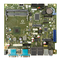
Copyright © 2014 congatec AG IGX1m02 44/134
Parameter Range
GPI/O Input Low Voltage -0.5V … 0.8V
GPI/O Input High Voltage 2V … 3.3V
GPI/O Output Low Voltage max. 0.7V
GPI/O Output High Voltage min. 2.5V
Note
Maximum load per GPI/O pin: 10mA (overall current for all GPI/O pins must be < 85mA) Each GPI/O pin has an integrated serial resistor of 150
Ohm. GPIO access is provided via the SM-Bus controller PCA9554A. SM-Bus address: 0x78h (8-bit).
7.2 Internal USB 2.0 Ports
Pin Signal Pin Signal
1 VCC AUX 2 VCC AUX
3 Data negative Port X 4 Data negative Port Y
5 Data positive Port X 6 Data positive Port Y
7 GND 8 GND
9 Key 10 Not connected
Pin Signal
1 VCC auxiliary
2 Data negative
3 Data positive
4 GND
Fused with polyswitch and power supervision with over current detection
Note
External USB sticks may cause EMI/ESD issues. This can be avoided by using the internal USB port for the affected stick.
Drive Po
LVDS
CPU
Memory Module 1
Memory Module 2
BIOS Recovery Settings
LVDS Supply Settings
USB 2.0
LVDS BL Control Settings
System Power On Settings
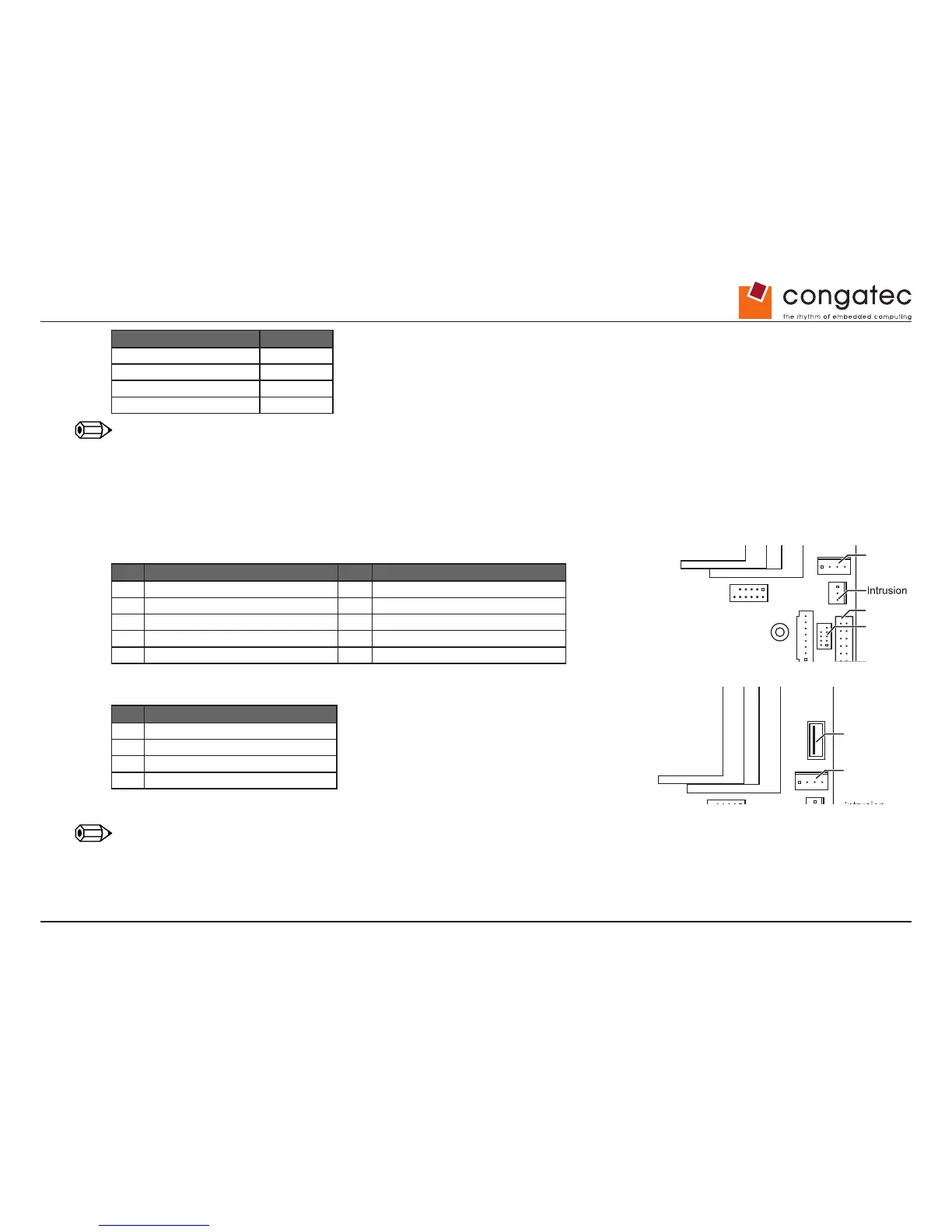
1
1
Fan 1 (CPU)
1 = GND
2 = 12 V PWM mode, 4..12 V 3-pin mode
3 = Sense
4 = PWM
1
Fan 2 (Chassis)
4
2
3
2
1
DC DVI-I DisplayPort
COM1 COM2
BIOS Recovery Settings
Normal Operation (default)
Normal Operation (default)
LVDS Supply Settings
LVDS BL Control Settings
System Power On Settings
Always on
BIOS Recovery / Reset to Defaults
VCC 3.3 V
(default)
VCC 5 V
Analog
(default)
PWM
LVDS BL Control Settings
System Power On Settings
1
1
Fan 1 (CPU)
1 = GND
2 = 12 V PWM mode, 4..12 V 3-pin mode
3 = Sense
4 = PWM
1
Fan 2 (Chassis)
4
2
3
2
1
DC DVI-I DisplayPort
COM1 COM2
BIOS Recovery Settings
Normal Operation (default)
Normal Operation (default)
LVDS Supply Settings
LVDS BL Control Settings
System Power On Settings
Always on
BIOS Recovery / Reset to Defaults
VCC 3.3 V
(default)
VCC 5 V
Analog
(default)
PWM