Safety
Information
Introduction
Product
Information
System
configuration
Mechanical
Installation
Electrical
Installation
Getting
Started
Basic
parameters
Running
the motor
Optimization
SMARTCARD
operation
Onboard
PLC
Advanced
parameters
Technical
Data
Diagnostics
UL Listing
Information
Unidrive SPM User Guide 243
Issue Number: 3 www.controltechniques.com
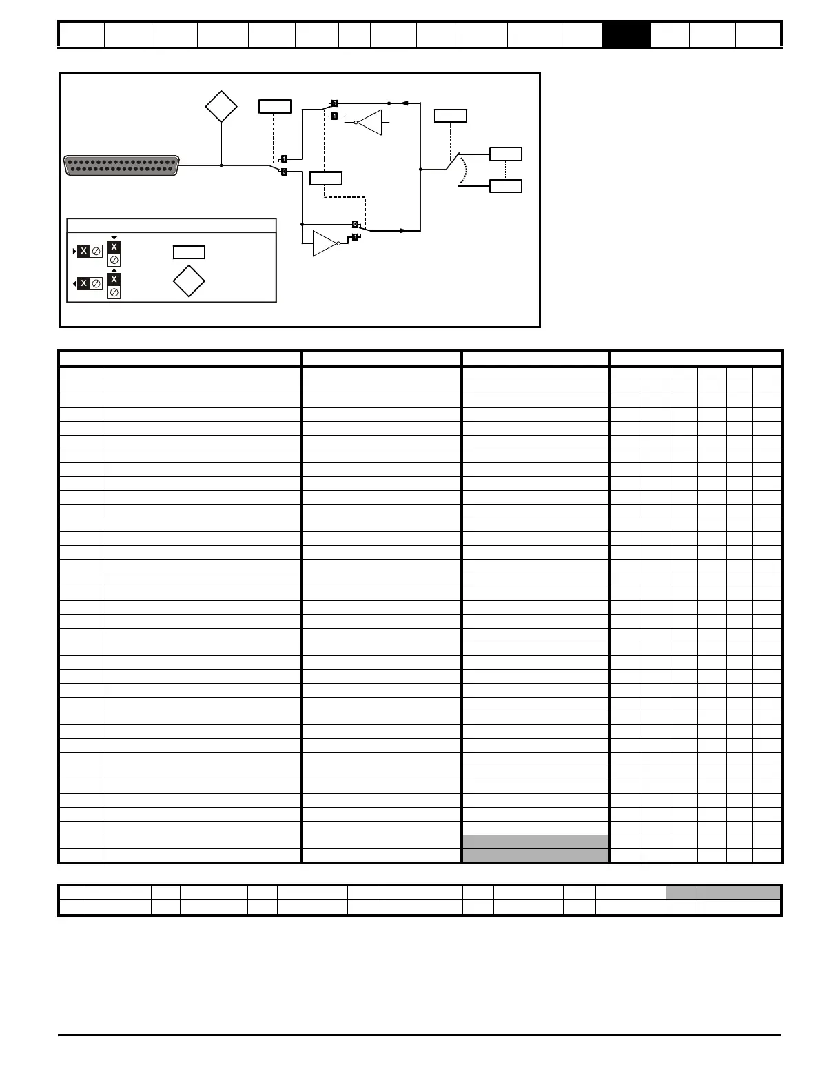
Figure 13-6 SM-I/O 32 logic diagram
SM-I/O 32 parameters
*See trip SLX.Er, Automation (I/O Expansion) module category
on page 286
.
X.XX
X.XX
Key
Read-write (RW)
parameter
Read-only (RO)
parameter
Input
terminals
Output
terminals
The parameters are all shown at their default setting
X.3y*
x(-1)
x(-1)
X.1y
X.0y**
I/O state
Output
select
Source/
destination
I/O invert
X.2y
Any unprotected
parameter
Parameter Range(Ú) Default(Ö)Type
x.01
Solutions Module ID code 0 to 599 208 RO Uni PT US
x.02 Solutions Module main software version 0.00 to 99.99 99.00 RO Uni NC PT
x.03 Digital I/O 3 state OFF(0) or On(1) OFF (0) RO Bit NC PT
x.04 Digital I/O 4 state OFF(0) or On(1) OFF (0) RO Bit NC PT
x.05 Digital I/O 5 state OFF(0) or On(1) OFF (0) RO Bit NC PT
x.06 Digital I/O 6 state OFF(0) or On(1) OFF (0) RO Bit NC PT
x.07 Digital I/O 7 state OFF(0) or On(1) OFF (0) RO Bit NC PT
x.08 Digital I/O 8 state OFF(0) or On(1) OFF (0) RO Bit NC PT
x.09 Digital I/O 1 state OFF(0) or On(1) OFF (0) RO Bit NC PT
x.10 Digital I/O 2 state OFF(0) or On(1) OFF (0) RO Bit NC PT
x.11 Digital I/O 1 invert OFF(0) or On(1) OFF (0) RW Bit US
x.12 Digital I/O 2 invert OFF(0) or On(1) OFF (0) RW Bit US
x.13 Digital I/O 3 invert OFF(0) or On(1) OFF (0) RW Bit US
x.14 Digital I/O 4 invert OFF(0) or On(1) OFF (0) RW Bit US
x.15 Digital I/O 5 invert OFF(0) or On(1) OFF (0) RW Bit US
x.16 Digital I/O 6 invert OFF(0) or On(1) OFF (0) RW Bit US
x.17 Digital I/O 7 invert OFF(0) or On(1) OFF (0) RW Bit US
x.18 Digital I/O 8 invert OFF(0) or On(1) OFF (0) RW Bit US
x.20 Digital I/O read word 0 to 255 0 RO Uni NC PT
x.21 Digital I/O 1 source/destination Pr 0.00 to Pr 21.51 Pr 0.00 RW Uni DE PT US
x.22 Digital I/O 2 source/destination Pr 0.00 to Pr 21.51 Pr 0.00 RW Uni DE PT US
x.23 Digital I/O 3 source/destination Pr 0.00 to Pr 21.51 Pr 0.00 RW Uni DE PT US
x.24 Digital I/O 4 source/destination Pr 0.00 to Pr 21.51 Pr 0.00 RW Uni DE PT US
x.25 Digital I/O 5 source/destination Pr 0.00 to Pr 21.51 Pr 0.00 RW Uni DE PT US
x.26 Digital I/O 6 source/destination Pr 0.00 to Pr 21.51 Pr 0.00 RW Uni DE PT US
x.27 Digital I/O 7 source/destination Pr 0.00 to Pr 21.51 Pr 0.00 RW Uni DE PT US
x.28 Digital I/O 8 source/destination Pr 0.00 to Pr 21.51 Pr 0.00 RW Uni DE PT US
x.29 Digital I/O 4 output select OFF(0) or On(1) On(1) RW Bit PT US
x.31 Digital I/O 1 output select OFF(0) or On(1) OFF (0) RW Bit US
x.32 Digital I/O 2 output select OFF(0) or On(1) OFF (0) RW Bit US
x.33 Digital I/O 3 output select OFF(0) or On(1) OFF (0) RW Bit US
x.43 First update method direction register Pr 0.00 to Pr 21.51 Pr 0.00 RW Uni DE PT US
x.47 Fast update method read register Pr 0.00 to Pr 21.51 Pr 0.00 RW Uni DE PT US
x.48 Fast update method write register Pr 0.00 to Pr 21.51 Pr 0.00 RW Uni PT US
x.50 Solutions Module error status* 0 to 255 RO Uni NC PT
x.51 Solutions Module software sub-version 0 to 99 RO Uni NC PT
RW Read / Write RO Read only Uni Unipolar Bi Bi-polar Bit Bit parameter Txt Text string
FI Filtered DE Destination NC Not copied RA Rating dependent PT Protected US User save PS Power down save
 Loading...