Home
Neoway
Network Hardware
N715-EA
Page 12 (Physical Features and Specifications)
Neoway N715-EA - Physical Features and Specifications
86 pages
Manual
Save Page as PDF
To Next Page
To Next Page
To Previous Page
To Previous Page
Loading...
N715-
EA
Hardware User Guide
Chapter
2
About N715-
EA
Copyright © Neoway
T
echnology Co., Ltd
12
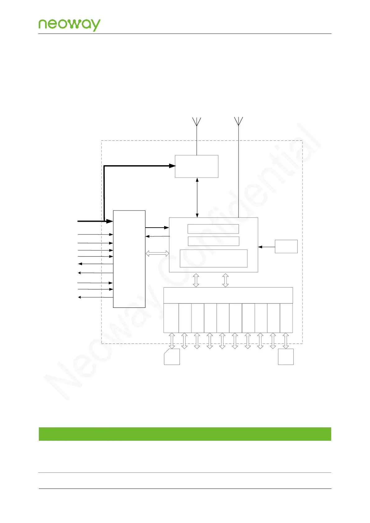
⚫
Radio frequency
⚫
Digital interfaces (USIM, I2C, SPI, KEYP
AD, UART
, USB, SDIO, PCM, and LCD)
⚫
Analog interfaces (ADC, MIC, ERA, SPK, HEADSET)
Fi
gur
e
2-1
Bl
oc
k d
iag
ra
m
UA
RT
VBA
T
Powe
r
ma
n
age
r
26
MHz
cryst
al
RF
fro
nt-
end
US
IM
Dig
ital in
terface
AN
T_MAIN
AN
T_WLAN
_
BT
PWR
KEY_
N
RE
SET_N
M
IC
AD
C
RF tra
ns
c
eiv
er
Bas
eb
and
NO
R
fl
ash (
64
Mb
) + PSR
AM
(
128
Mb
)
SPK
EAR
PC
32
kHz
c
l
oc
k
Con
trol
HE
ADSE
T
Cha
rge
VD
D_1P8
SPI
SD
IO
LCD
CA
M
KEY
PAD
I2C
PC
M
US
B
US
IM
2.3
Basic Features
Parameter
Description
Physical features
⚫
Dimensions: (23.80±
0.1) mm ×
(22.80±
0.1) mm ×
(2.5±
0.15) mm
⚫
Package: 76-pin LCC + 72-pin LGA
⚫
Weight: TBD
11
13
Table of Contents
Main Page
Default Chapter
3
Table of Contents
3
1 Safety Recommendations
10
2 About N715-EA
11
Product Overview
11
Block Diagram
11
Table 2-1 Variants and Frequency Bands
11
Basic Features
12
Figure 2-1 Block Diagram
12
3 Reference Standards
15
4 Module Pins
16
Pad Lay-Out
16
Figure 4-1 N715-EA Pad Lay-Out (Top View)
16
Pin Descriptions
17
Table 4-1 IO Definitions and DC Characteristics
17
Table 4-2 Pin Descriptions
18
5 Application Interfaces
28
Power Interfaces
28
Vbat
28
Figure 5-1 Voltage Drops of the Power Supply
29
Figure 5-2 Recommended Design 1
30
Figure 5-3 Recommended Design 2
30
Figure 5-4 Recommended Design 3
31
Figure 5-5 Recommended Design 4
32
Vdd_1P8
33
Control Interfaces
33
Power-On
33
Table 5-1 Module Power-On Descriptions
33
Figure 5-6 Reference Design of Power-On Controlled by a Button
34
Figure 5-7 Reference Design of Power-On Controlled by an MCU
35
Figure 5-8 Power-On Process
35
Power-Off
36
Figure 5-9 Reference Design of Automatic Power-On Once Powered-Up
36
Reset
37
Figure 5-10 Hard Power-Off Process
37
Figure 5-11 Reference Design for Reset by Using a Button
38
Figure 5-12 Reference Design for Reset Controlled by an MCU
38
Peripheral Interfaces
39
Usb
39
Figure 5-13 Reset Process of the N715-EA Module
39
Uart
40
Figure 5-14 Recommended Design of the USB Interface
40
Figure 5-15 Reference Design of UART Interface
41
Figure 5-16 Recommended Voltage-Level Translation Circuit1
42
Figure 5-17 Recommended Voltage-Level Translation Circuit 2
43
Usim
44
Figure 5-18 Recommended Voltage-Level Translation Circuit 3
44
Figure 5-19 Reference Design of the USIM Card Interface (Normally Closed Type)
45
Figure 5-20 Reference Design of the USIM Card Interface (Normally Open Type)
46
Sdio
47
Figure 5-21 Reference Design of the USIM Card (Without Hot-Swap) Interface
47
Sdcard (Signal Multiplexing)
48
Pcm
49
Figure 5-22 Reference Design of the SD Card Interface
49
Spi
50
Figure 5-23 PCM Reference Design
50
I2C
51
Figure 5-24 SPI Reference Design
51
Figure 5-25 I2C Reference Design
51
Audio Interfaces
52
Analog Audio Input
52
Figure 5-26 Reference Design of the MIC Differential Input
52
Analog Audio Output
53
Figure 5-27 Reference Design of Audio Interface in EAR/ SPK Differential Mode
54
Headset Interface
55
Figure 5-28 Reference Design of the External Power Amplifier Connection
55
Table 5-2 Headset Audio Pin Description
55
Figure 5-29 Reference Design of the Headset Interface
56
Figure 5-30 Headphone Interface Diagram
57
Video Interfaces
58
Lcd
58
Table 5-3 LCD Interface Pin Description
58
Camera
59
Radio Frequency
59
Ant_Mainantenna Interfaces
59
Figure 5-31 L-Type Network
60
Figure 5-32 T-Type Network
60
Figure 5-33 Π-Type Network
60
Ant_Wlan_Bt
61
Antenna Assembling
61
Figure 5-34 Recommended RF PCB Design
61
Figure 5-35 Murata RF Connector Encapsulation Specifications
62
Figure 5-36 RF Cable Connections
62
Figure 5-37 Antenna Layout
63
Figure 5-38 Layout Around the Antenna
63
GPIO Interfaces
64
Multi-Function Interfaces
64
Table 5-4 Pin Definition Description
64
Other Interfaces
65
Adc
65
Wakeup_In
65
Figure 5-39 Process of Entering into Sleep Mode
66
Figure 5-40 Incoming Call Service Process
66
Figure 5-41 Outgoing Call Service Process
67
Figure 5-42 Process of Existing from Sleep Mode
67
Status Indication
68
Figure 5-43 Driving LED Indicator with a Triode
68
Usb_Boot
69
Keypad
69
Figure 5-44 Reference Design of USB Emergency Download Mode
69
PSM Interface
70
6 Electrical Characteristics and Reliability
71
Electrical Characteristics
71
Table 6-1 N715-EA Electrical Characteristics
71
Table 6-2 N715-EA Current Consumption (Typical)
71
Temperature Characteristics
72
ESD Protection
72
Table 6-3 N715-EA Temperature Characteristics
72
Table 6-4 N715-EA ESD Protection Characteristics
72
7 RF Characteristics
73
Operating Band
73
TX Power and RX Sensitivity
73
Table 7-1 N715-EA Operating Bands
73
Table 7-2 N715-EA RF Transmit Power
73
Table 7-3 RF RX Sensitivity of N715-EA
74
WLAN/BT Characteristics
75
Table 7-4 WLAN/BT TX Power and RX Sensitivity
75
8 Mechanical Characteristics
76
Dimensions
76
Figure 8-1 N715-EA Top and Side View Dimensions (Unit: MM)
76
Label
77
Packaging
77
Reels
77
Moisture Sensitivity Level
79
9 Mounting
81
PCB Package
81
Figure 9-1 Bottom View of N715-EA PCB Package (Unit: MM)
81
Application PCB Package
82
Figure 9-2 N715-EA Application PCB Package (Top View, Unit: MM)
82
Stencil
83
Solder Paste
83
SMT Oven Temperature Profile
83
Figure 9-3 Oven Temperature Profile
84
Abbreviations
85