PCB Design Guidelines
⚫
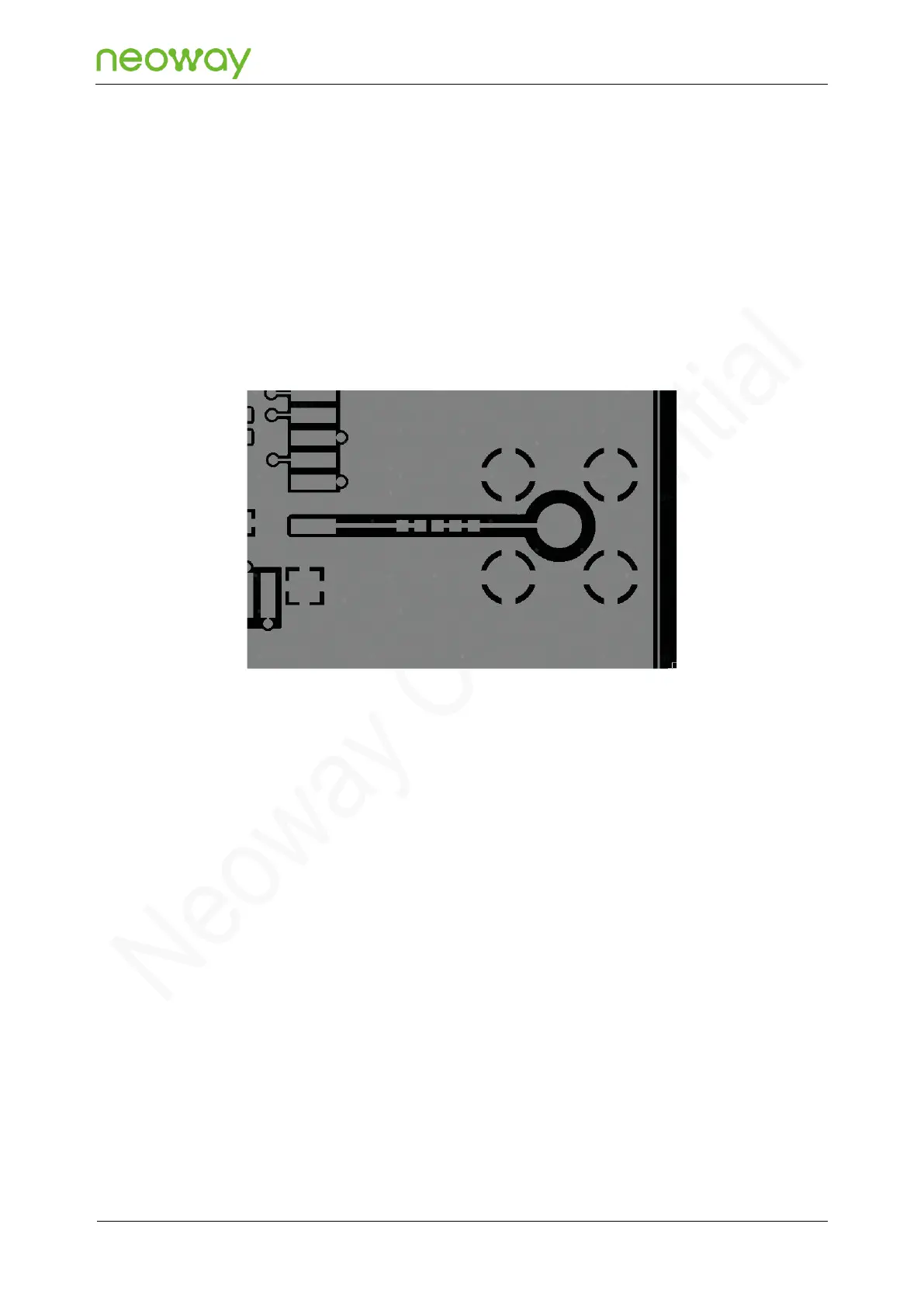
Lay copper foil around the RF connector. Dig as many ground holes as possible on the copper
and the characteristic impedance of all RF traces should be controlled to 50 Ω.
⚫
Traces between the RF pin and the antenna connector should be as short as possible. Control
the trace impedance to 50 Ω.
⚫
If you adopt an SMA connector, a big RF solder pad might result in great parasitic capacitance,
which will affect the antenna performance. Remove the copper on the first and fourth layers or all
layers of a multiple-layer PCB under the RF solder pad.
Figure 5-34 Recommended RF PCB design
⚫
A reasonable distance should be kept between ANT_MAIN and ANT_WLAN_BT to avoid mutual
interference that may affect reception performance.
⚫
On the PCB, keep the RF signals and components far away from high-speed circuits, power
supplies, transformers, great inductors, the clock signal, etc.
5.6.2 ANT_WLAN_BT
The 42 pin of the N715-EA module is shared by the WLAN and Bluetooth antennas. It has a
characteristic impedance of 50 Ω.
For the schematic design and the PCB design of the WLAN antenna and Bluetooth antenna interface,
see the requirements in section 5.6.1 “ANT_MAIN”.
5.6.3 Antenna Assembling
The antenna used by the module must comply with the mobile device standard. The standing wave
ratio should be between 1.1 and 1.5, and the input impedance should be 50 Ω. Requirements for
antenna gain vary according to the application environment. You can choose a suitable antenna
according to specific application scenarios and environments.