N715-EA Hardware User Guide
Chapter 5 Application Interfaces
Copyright © Neoway Technology Co., Ltd. All rights reserved.
Do Not directly apply the parameter values of the components provided by the circuit to your circuit design;
they need to be adjusted according to the actual situations. Note the difference between different voltage-level
translation circuits .
⚫
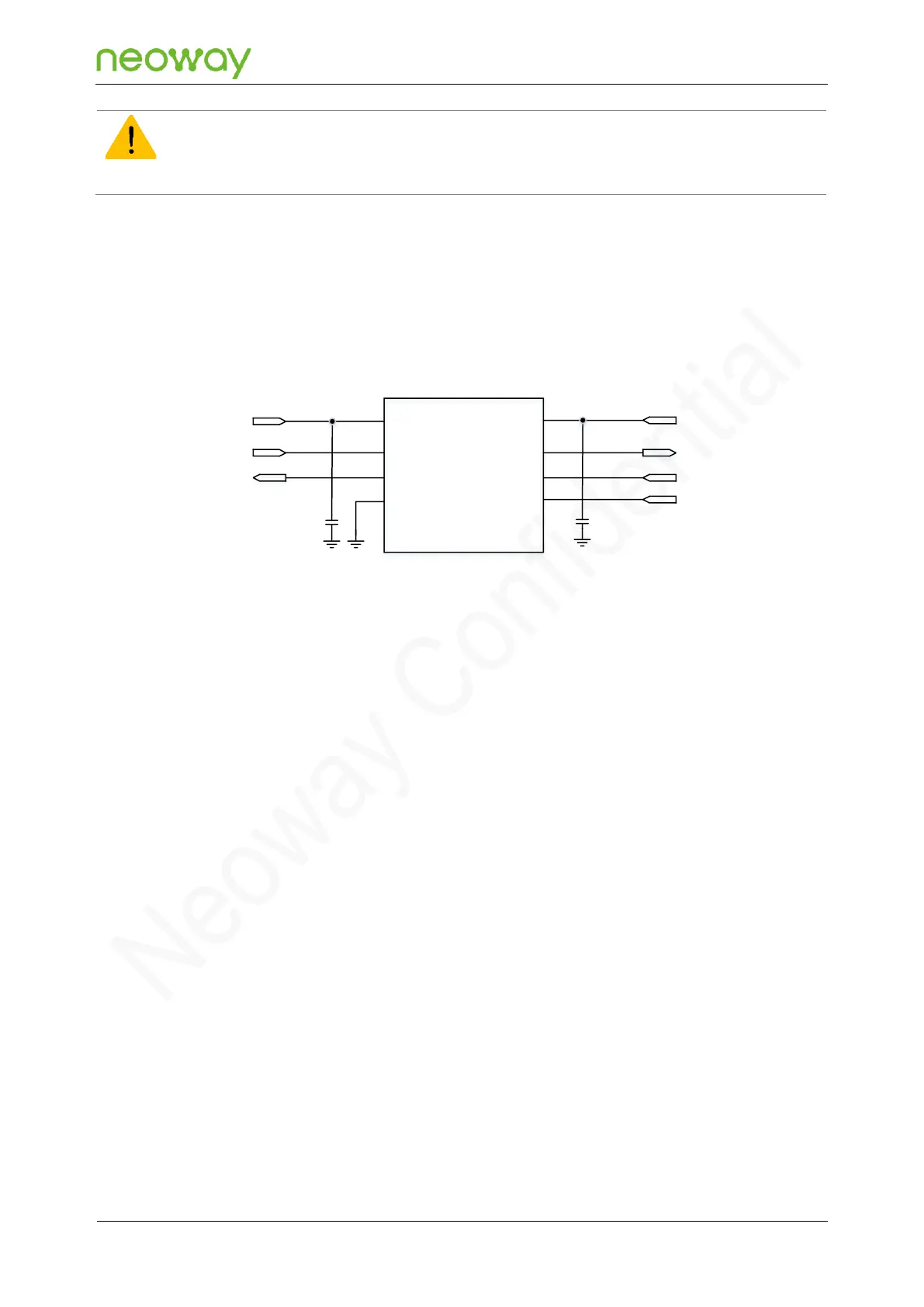
Voltage-Level Translation Circuit (Translator Chip)
If the UART baud rate is greater than 115200 bps, it is recommended to refer to the
recommended voltage-level translation circuit 1. See Figure 5-16.
Figure 5-16 Recommended voltage-level translation circuit1
VL
IO_VL1
IO_VL2
GND
VCC
IO_VCC1
IO_VCC2
EN
VDD_1P8
UART_TXD
UART_RXD
C1
0.1uF
VCC_IO
MCU_RXD
MCU_TXD
C2
0.1uF
VDD_1P8
− VL is the reference voltage of IO_VL1 and IO_VL2, ranging from 1. 5 V to 5.5 V.
− VCC is the reference voltage of IO_VCC1 and IO_VCC2, ranging from 1. 5 V to 5.5 V.
− EN is the enable pin, which works at a voltage of greater than VL-0.2 V. In the above circuit,
the EN pin is connected to VDD_1P8 and the translator chip is always working.
⚫
Dual-triode Voltage-Level Translator Circuit
If the serial port baud rate is less than or equal to 115200 bps, design the serial port TXD and
RXD by referring to recommended voltage-level translation circuit 2. As shown in Figure 5-17.