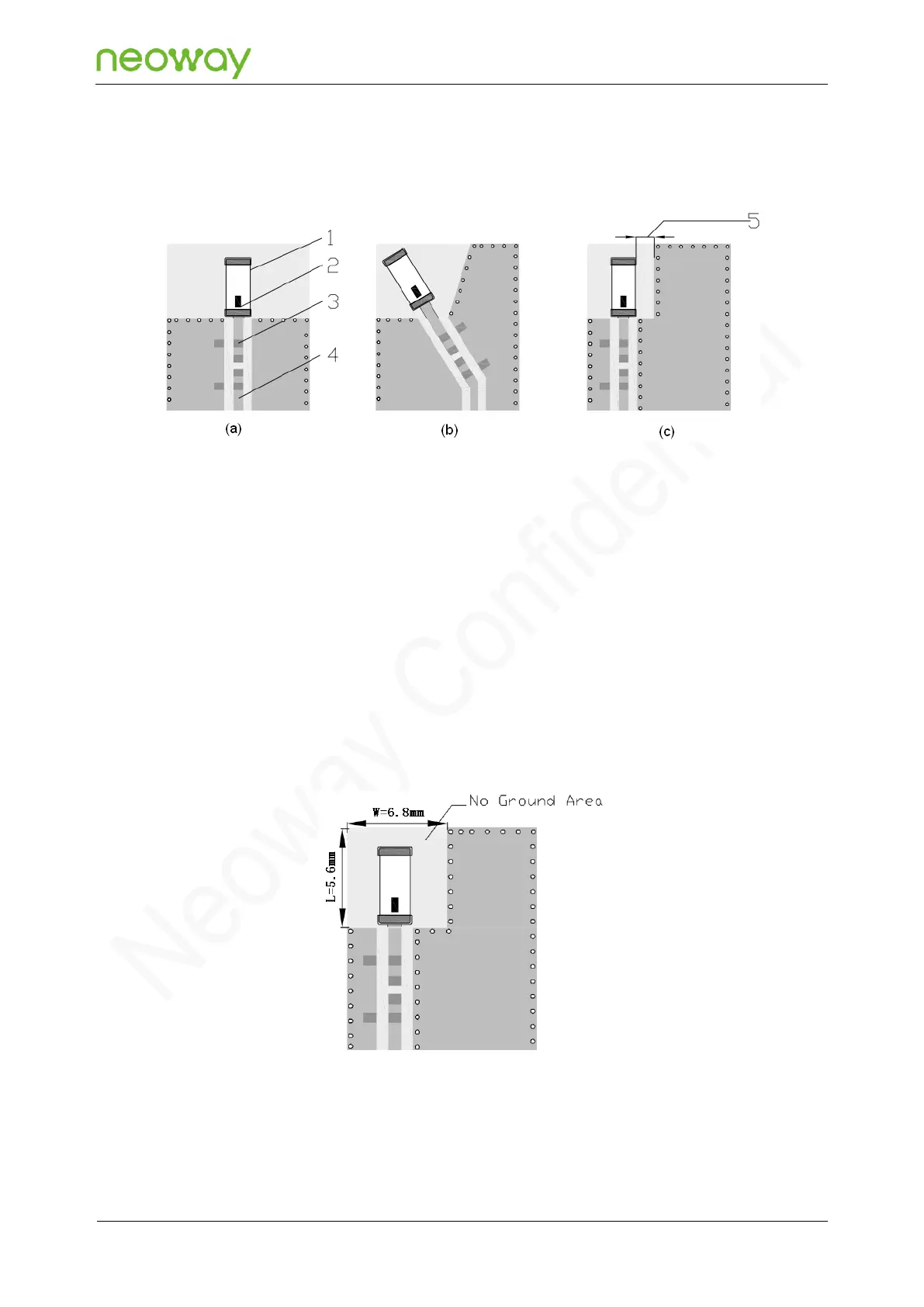
The following figure shows the layout of the 2.4 GHz ceramic chip antenna. SLDA52-2R540G-S1TF is
used as an example.
Figure 5-37 Antenna layout
If your PCB is large enough, you can adopt the layout shown in Figure 5-37 (a).
⚫
1 Chip antenna
⚫
2 Feeding mark
⚫
3 Layout pad of the matching circuit
⚫
4 50 Ω characteristic impedance RF traces
Figure 5-38 shows the layout for the area between the antenna and ground that is marked as "5" in
Figure 5-37.
Figure 5-38 Layout around the antenna
For more details, refer to the antenna manuals and other documents.