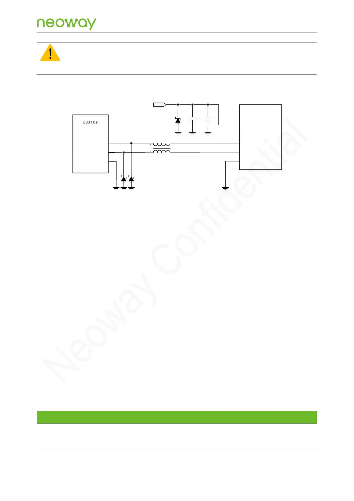
The reverse current may flow from the USB powering device to the VBAT circuit (around 2.5 V) when VBAT is
powered down. To prevent the reverse current from affecting the total circuit design, it is recommended that you
add a power switch for the USB_VBUS power.
Schematic Design Guidelines
⚫
Connect a 1 μF (C1) and a 33 pF (C2) filter capacitor in parallel to the USB_VBUS pin. An ESD
component must be added for the power cable.
⚫
The junction capacitance of the ESD components D2 and D3 on the USB_DP and USB_DM
cables must be smaller than 0.5 pF.
⚫
To improve EMI interference generated by USB signals, connect a common-mode inductor L1 to
the USB_DP and USB_DM cables in series.
PCB Design Guidelines
⚫
Place the filter capacitor on the USB_VBUS as close to the module pins as possible and place
the ESD component as close to the USB connector as possible.
⚫
Place the ESD component on the USB_DP and USB_DM cables as close to the USB connector
as possible.
⚫
It is important to route the USB signal traces as differential pairs. The impedance of USB
differential trace is 90 Ω. The cable from the USB host to the module must be isolated from other
signal cables with ground surrounded.
5.3.2 UART