Schematic Design Guidelines
⚫
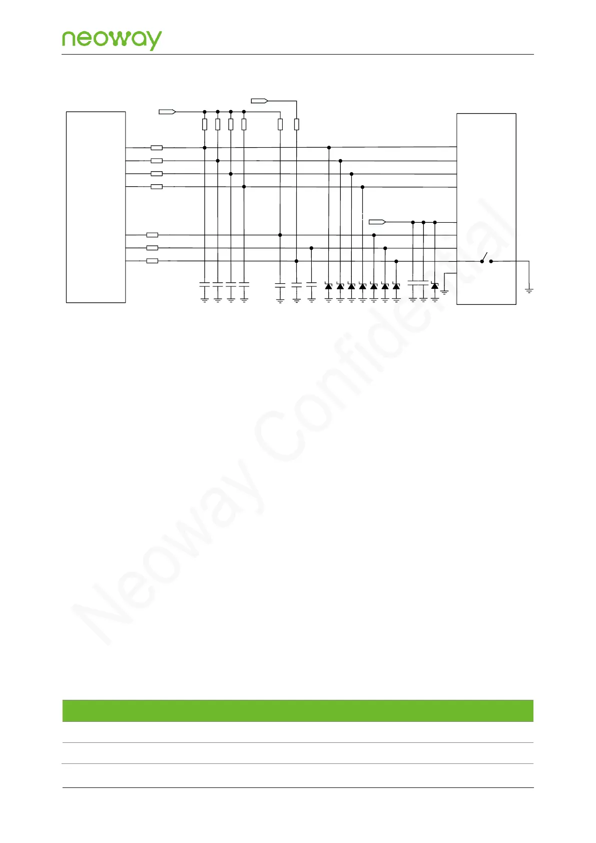
VDD_SDCPULL is a 1.8 V/3.0 V dual-voltage power supply; configure it according to the SD
card voltage type. It outputs a maximum current of 50 mA and is only used for SD pull-up. Do not
use it for any other purpose.
⚫
SD_VDD is used to drive SD card peripherals
⚫
N715-EA supports SD card detection, which is triggered by a 1.8 V interrupt pin. The SD
detection circuit works by checking the voltage-level across the USIM_DET pin before and after
a SD card is inserted. In the reference circuit, Figure 5-22, SD_DET is at a high-level voltage
(with external pull-up to VDD_1P8) before a SD card is inserted and is grounded after a SD card
is inserted. The low-level means SD card detected while the high-level means no SD card
detected.
PCB Design Guidelines
⚫
Ensure that the power supply trace width is not less than 0.6 mm.
⚫
Control the trace lengths of each SDIO signal. The DATA traces should be matched in length to
within 0.5 mm, and the CMD, CLK and DATA traces should be matched in length to within 0.5
mm.
⚫
Spacing between DATA traces should be larger than 2 times trace width.
⚫
Control the impedance for each SDIO trace to 50 Ω.
5.3.6 PCM