Reference Design without External Power Amplifier
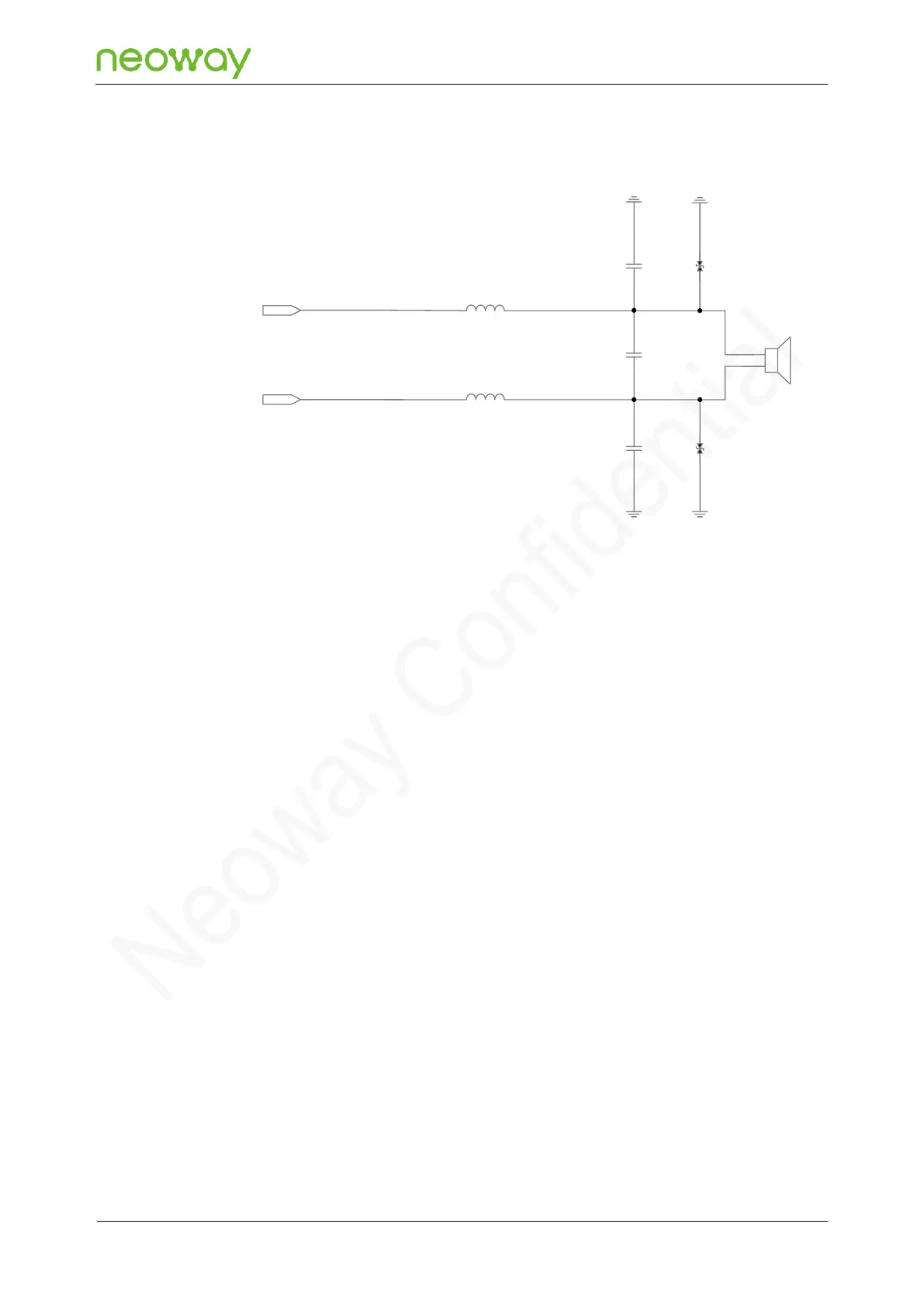
Figure 5-27 Reference design of audio interface in EAR/ SPK differential mode
Schematic Design Guidelines
⚫
C2, C3, and C4 are used to place capacitors to filter out jamming frequencies.
⚫
TVS diodes at D1 and D2 are used to prevent ESD from damaging the module.
⚫
B1 and B2 are ferrite beads to filter out high-frequency noise. It is recommended to use ferrite
beads specifically for audio.
Note the DC resistance of the ferrite beads because overlarge DC resistance will consume too
much audio power while audio output components generally have a small impedance. A ferrite
bead with a DC resistance lower than 0.1 Ω is recommended.
PCB Design Guidelines
⚫
The audio signal traces should be wide enough (0.5 mm is recommended) on the PCB to bear
large current when audios are outputted at the highest volume. Isolate the traces from high-
speed digital signals and clocks as well as other analog signal traces. No signal trace crossing is
allowed. Reserve enough grounding holes and ground protection.
⚫
Keep audio traces far away from antenna to reduce jamming. Avoid parallel layout between
power supply traces and audio traces.
⚫
It is important to route the audio signal traces as differential pairs.