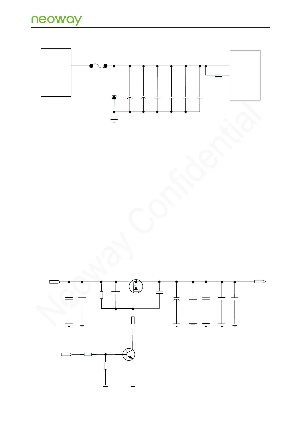
⚫
The maximum input voltage for the module is 4.2 V and the typical value is 3.6 V.
⚫
The reverse voltage across D1 (a TVS diode) should be 4.5 V (V
RWM
=4.5V) and the peak power
(Ppp) should be 2800 W (tp=8/20uS). Keep the placement of the TVS diode close to the power
input interface to suppress the surge voltage before it enters back-end circuits to prevent the
back-end component and the module from damaging.
⚫
To decrease voltage drops during bursts, a large bypass tantalum capacitor (220 μF or 100 μF)
or aluminum capacitor (470 μF or 1000 μF) is expected at C1 and C2. Its maximum safe
operating voltage should be larger than 2 times the voltage across the power supply.
⚫
To get a stable power source, place a bypass capacitor (C3, C4, C5, and C6) of low-ESR close
to the VBTA pins to filter out high-frequency jamming.
The following circuit design is recommended to control the power supply.
Figure 5-3 Recommended design 2