Schematic Design Guidelines
⚫
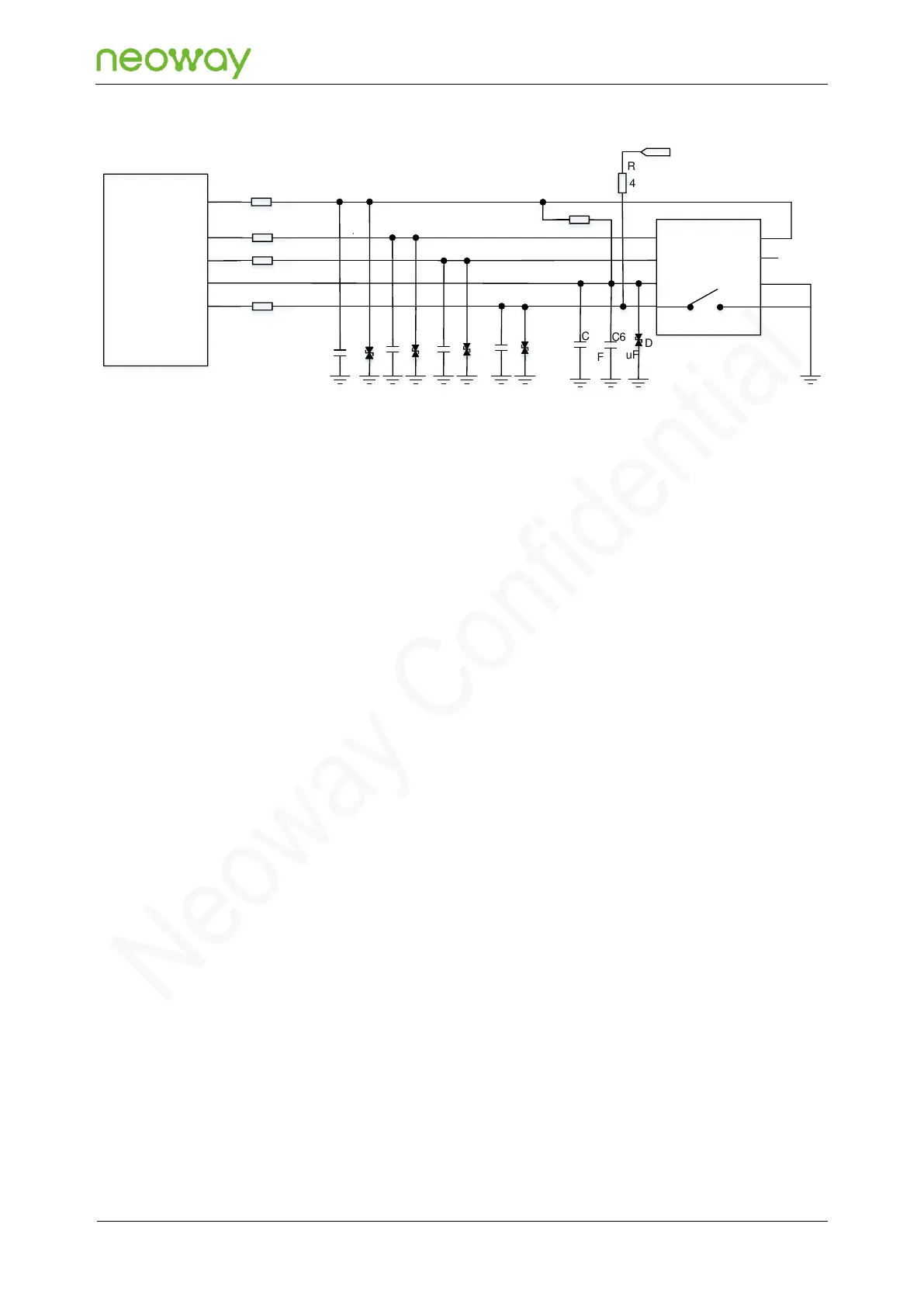
USIM_VCC is the pin to supply power for USIM card and its maximum load is 50 mA. It is only
used as power supply for USIM card (forbidden to supply power to other loads).
⚫
Connect the USIM_DATA pin to USIM_VCC through a 4.7 kΩ resistor since there is no pull-up
inside USIM_DATA.
⚫
USIM_CLK is the clock signal pin of the USIM card. In applications with complex
electromagnetic environments that have high requirements for ESD protection, it is
recommended to add ESD protection diodes (junction capacitance ≤ 7pF) on each signal cable
or add an integrated ESD component.
⚫
Connect a resistor (not greater than 20 Ω) respectively to USIM_DATA, USIM_RESET,
USIM_CLK, and USIM_DET (close to the card connector) in series to enhance the ESD
performance.
⚫
The placements from C1 to C4 are designed to place the high-frequency filter capacitors. The
recommended capacitance value is not greater than 10 pF. No capacitors are placed on them by
default in design. Please adjust it according to the actual debugging results.
⚫
N715-EA supports USIM detection. USIM_DET is a 1.8 V interrupt pin. The USIM detection
circuit works by checking the voltage-level across the USIM_DET pin before and after a USIM
card is inserted. In the reference circuit, Figure 5-19, SIM_DET is grounded before a USIM card
is inserted and is connected to a 1.8 V voltage after a USIM card is inserted. The high voltage-
level means USIM card detected while the low voltage-level means no USIM card detected. In
the reference circuit, Figure 5-20, SIM_DET is at a high-level voltage before a USIM card is
inserted and is grounded after a USIM card is inserted. The low voltage-level means USIM card
detected while the high voltage-level means no USIM card detected.