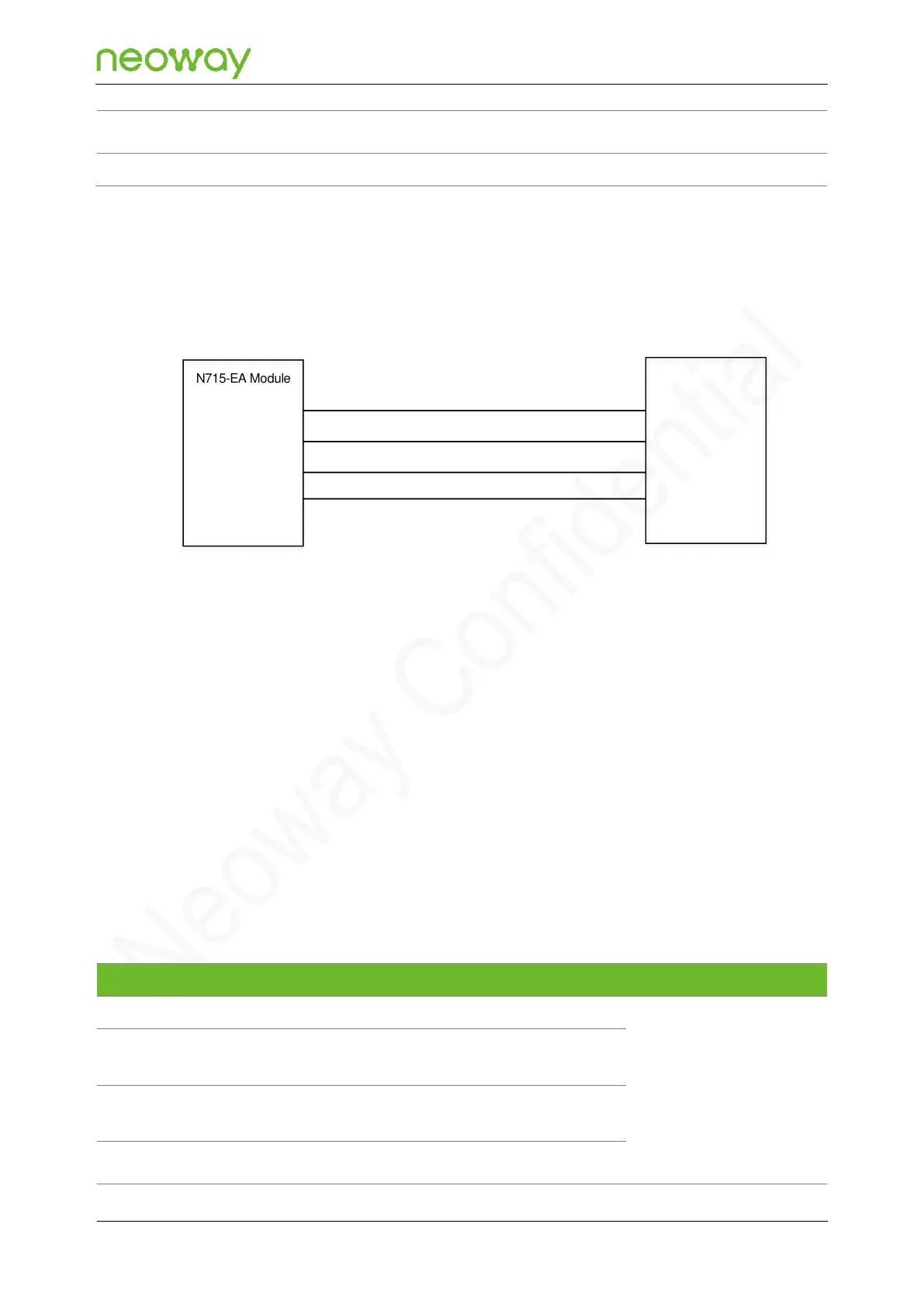
N715-EA provides one 1.8 V PCM interface. The following figure shows the reference design of the
PCM interface.
Figure 5-23 PCM reference design
Schematic Design Guidelines
If the levels of N715-EA and Codec do not match, add a voltage-level translation circuit as required by
referring to the description of voltage-level translation circuit in section 5.3.2 .
PCB Design Guidelines:
⚫
Reduce the cross routing between the PCM signal cable and other cables. If cross routing
cannot be avoided, keep this signal cable perpendicular to other cables to reduce coupling.
⚫
Keep the PCM signal cable away from areas where static electricity may be introduced.
⚫
PCM_SCLK should be ground shielded. It is also recommended that other signal cables be
shielded with surrounded ground.
5.3.7 SPI