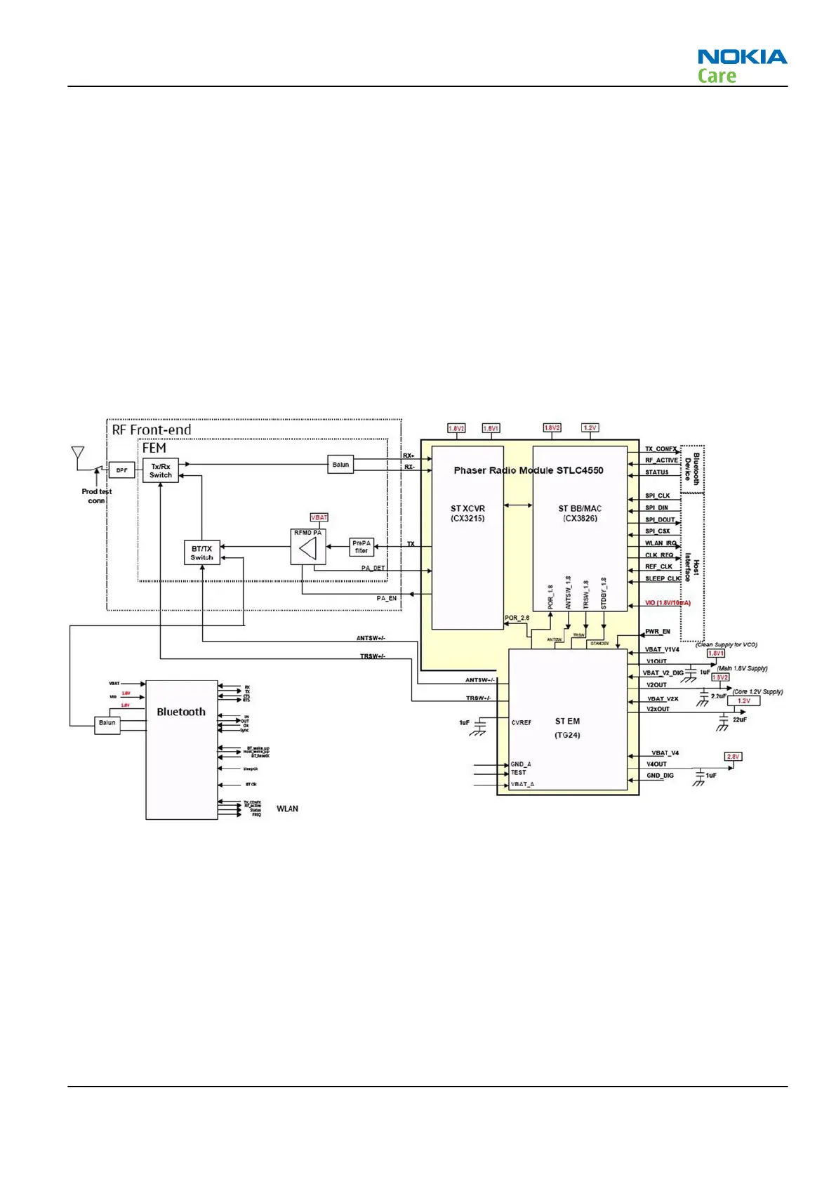
The energy management unit integrates required power management functions to operate the system from
VBAT (3.0 – 5.5 V). The EM unit generates 1.2 V digital core voltage, two 1.8 V supplies for RF and 2.8 V LDO
for PA bias supply. The EM unit also integrates power-on reset circuitry and level-shifters for RF front-end
GaAs switches.
Host interface is provided by a flexible serial interface (SPI) supporting clock frequency upto 48 MHz. The
maximum usable SPI clock rate depends on the host side clocking options and timing requirements. Typically
rates of 14 – 24 MHz are achieved. WLAN/BT coexistence interface enables automatic time shared usage of
WLAN and Bluetooth.
WLAN and Bluetooth systems use the same 38.4-MHz reference clock from Ritsa engine. The output signal
from Ritsa’s TCVCXO was tapped and buffered by a discrete clock buffer (V7400) and connected to WLAN and
BT’s reference clock inputs. Low power sleep mode or energy management stand-by state is enabled by using
32768-Hz speed clock.
WLAN RFMD RF5924 front end module is used. Power amplifier, RF-switches and baluns are integrated to
FEM. The PA includes power detector for closed-loop power control purposes. WLAN/BT bandpass filter is
external ceramic filter.
Figure 48 WLAN block diagram
RM-247
System Module
Issue 1 COMPANY CONFIDENTIAL Page 7 –15
Copyright © 2008 Nokia. All rights reserved.
 Loading...