167
Designating Command Parameters Section 5-2
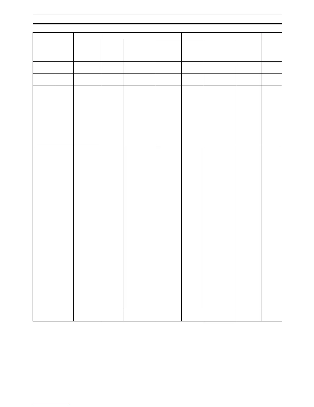
Note 1. The only current EM bank that can be read with FINS commands is the
current EM bank that is set at the end of the cycle.
2. On a CJ2 CPU unit only, 50 to 5F can be specified for the memory area
code of EM banks 0 to F.
Index
Register
IR PV DC IR00 to IR15 010000 to
010F00
--- --- --- 4
Data
Register
DR PV BC DR00 to
DR15
020000 to
020F00
9C DR0 to DR2 000300 to
000500
2
Clock Pulses Bit 07 1-min clock
pulse
1-s clock
pulse
0.2-s clock
pulse
0.1-s clock
pulse
0.02-s clock
pulse
000000
000100
000200
000300
000400
--- --- --- 1
Condition Flags Bit Error Flag
(ER)
Carry Flag
(CY)
Greater Than
Flag (>)
Equals Flag
(=)
Less Than
Flag (<)
Negative Flag
(N)
Overflow Flag
(OF)
Underflow
Flag (UF)
Greater Than
or Equals
Flag (>=)
Not Equal
Flag (<>)
Less Than or
Equals Flag
(<=)
Always OFF
Flag (ON)
Always ON
Flag (OFF)
100000
100100
100200
100300
100400
100500
100600
100700
100800
100900
100A00
100E00
100F00
--- --- 1
Access Error
Flag
200100 --- --- 1
Area Data type CS/CJ mode CV mode Length
per ele-
ment
Memory
area
code
(hex)
Memory area
address
Memory
address
Memory
area
code
(hex)
Memory area
address
Memory
address
 Loading...