173
FINS Commands Section 5-3
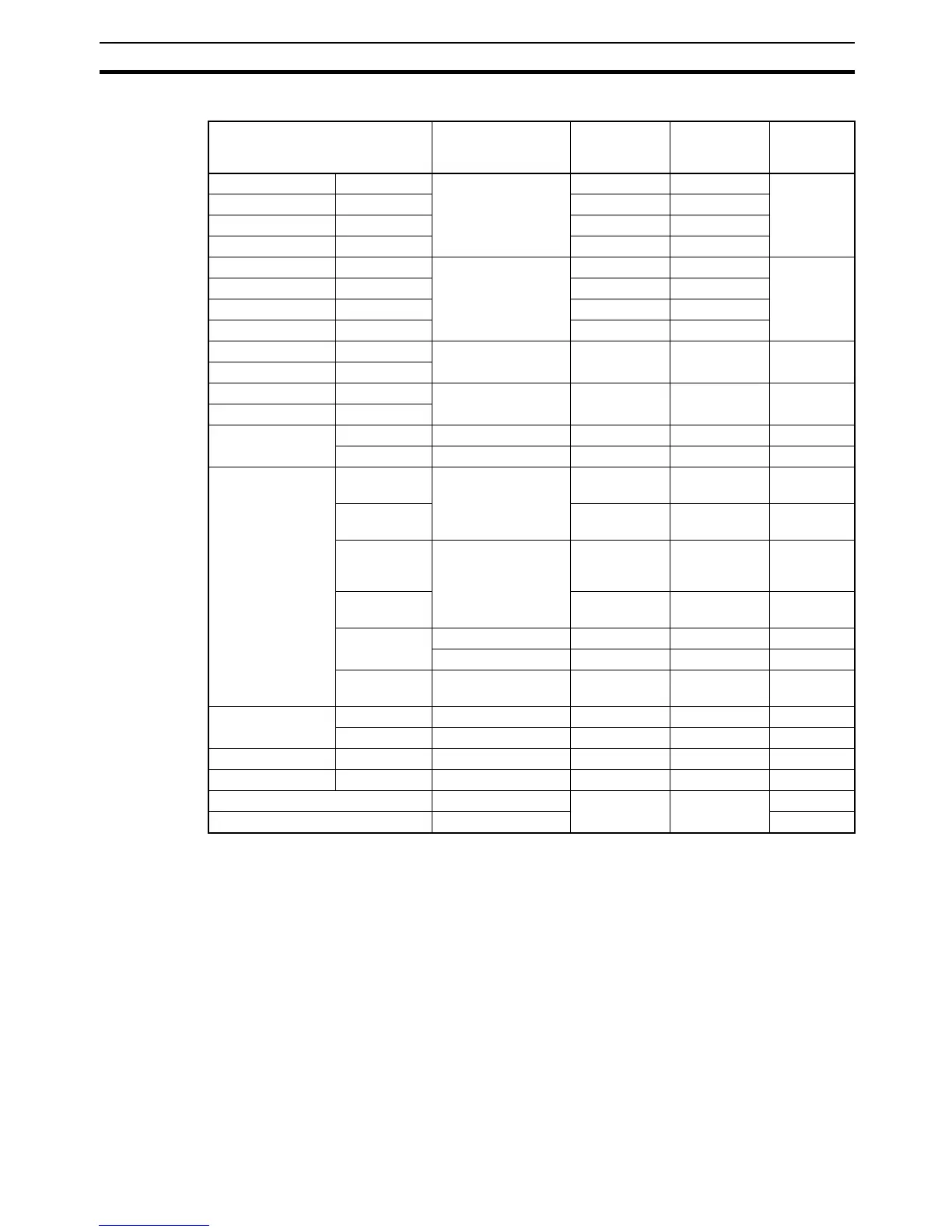
I/O Memory Area Codes
Note On a CJ2 CPU unit only, 50 to 5F can be specified for the memory area code
of EM banks 0 to F.
Area Data type CS/CJ mode
memory area
code (hex)
CV mode
memory area
code (hex)
Bytes per
element
CIO Area CIO Bit 30 00 1
Work Area WR 31 ---
Holding Bit Area HR 32 ---
Auxiliary Bit Area AR 33 00
CIO Area CIO Word B0 80 2
Work Area WR B1 ---
Holding Bit Area HR B2 ---
Auxiliary Bit Area AR B3 80
Timer Area TIM Completion Flag 09 01 1
Counter Area CNT
Timer Area TIM PV 89 81 2
Counter Area CNT
DM Area DM Bit 02 --- 1
DM Word 82 82 2
EM Area EM bank 0 to
bank F
Bit 20 to 2F --- 1
EM bank 10
to bank 18
E0 to E8 --- 1
EM bank 0 to
bank F
Word A0 to AF or
50 to 5F
(see note.)
90 to 97 2
EM bank 10
to bank 18
60 to 68 --- 2
EM current
bank
Bit 0A --- 1
Word 98 98 2
EM current
bank No.
Bank No. BC 9C 2
Task Flag TK Bit 06 --- 1
TK Status 46 --- 1
Index Register IR PV DC --- 4
Data Register DR PV BC 9C 2
Clock Pulses Bit 07 --- 1
Condition Flags Bit 1
 Loading...