RL78/G13 CHAPTER 29 ELECTRICAL SPECIFICATIONS
R01UH0146EJ0100 Rev.1.00 1011
Sep 22, 2011
Caution The pins mounted depend on the product. Refer to 2.1.1 20-pin products to 2.1.14 128-pin products,
and 2.1.15 Pins for each product (pins other than port pins).
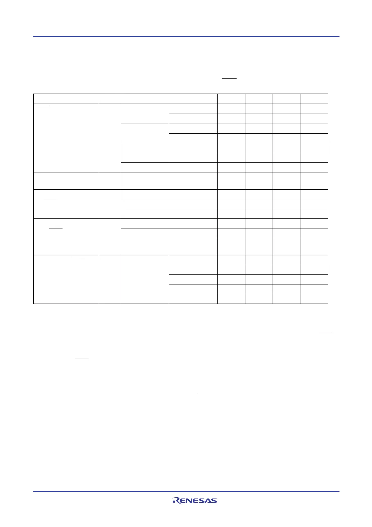
(4) During communication at same potential (CSI mode) (slave mode, SCKp... external clock input)
(T
A = −40 to +85°C, 1.6 V ≤ EVDD0 = EVDD1 ≤ VDD ≤ 5.5 V, VSS = EVSS0 = EVSS1 = 0 V)
Parameter Symbol Conditions MIN. TYP. MAX. Unit
20 MHz < fMCK 8/fMCK ns 4.0 V ≤ EVDD0 ≤ 5.5 V
fMCK ≤ 20 MHz 6/fMCK ns
16 MHz < fMCK 8/fMCK ns 2.7 V ≤ EVDD0 < 4.0 V
f
MCK ≤ 16 MHz 6/fMCK ns
16 MHz < fMCK 8/fMCK ns 1.8 V ≤ EVDD0 < 2.7 V
f
MCK ≤ 16 MHz 6/fMCK ns
SCKp cycle time
Note 5
tKCY2
1.6 V ≤ EV
DD0 < 1.8 V 6/fMCK ns
SCKp high-/low-level width
t
KH2,
t
KL2
1.6 V ≤ EV
DD0≤ 5.5 V tKCY2/2 ns
2.7 V ≤ EVDD0 ≤ 5.5 V 1/fMCK+20 ns
1.8 V ≤ EVDD0 < 2.7 V 1/fMCK+30 ns
SIp setup time
(to SCKp↑)
Note 1
t
SIK2
1.6 V ≤ EV
DD0 < 1.8 V 1/fMCK+40 ns
2.7 V ≤ EVDD0 ≤ 5.5 V 1/fMCK+31 ns
1.8 V ≤ EVDD0 < 2.7 V 1/fMCK+31 ns
SIp hold time
(from SCKp↑)
Note 2
t
KSI2
1.6 V ≤ EV
DD0 < 1.8 V
1/f
MCK+
250
ns
4.0 V ≤ EVDD0 ≤ 5.5 V 2/fMCK+44 ns
2.7 V ≤ EVDD0 < 4.0 V 2/fMCK+44 ns
2.4 V ≤ EVDD0 < 2.7 V 2/fMCK+75 ns
1.8 V ≤ EVDD0 < 2.4 V 2/fMCK+110 ns
Delay time from SCKp↓ to
SOp output
Note 3
t
KSO2 C = 30 pF
Note 4
1.6 V ≤ EV
DD0 < 1.8 V 2/fMCK+220 ns
Notes 1. When DAPmn = 0 and CKPmn = 0, or DAPmn = 1 and CKPmn = 1. The SIp setup time becomes “to SCKp↓”
when DAPmn = 0 and CKPmn = 1, or DAPmn = 1 and CKPmn = 0.
2. When DAPmn = 0 and CKPmn = 0, or DAPmn = 1 and CKPmn = 1. The SIp hold time becomes “from SCKp↓”
when DAPmn = 0 and CKPmn = 1, or DAPmn = 1 and CKPmn = 0.
3. When DAPmn = 0 and CKPmn = 0, or DAPmn = 1 and CKPmn = 1. The delay time to SOp output becomes
“from SCKp↑” when DAPmn = 0 and CKPmn = 1, or DAPmn = 1 and CKPmn = 0.
4. C is the load capacitance of the SOp output lines.
5. Transfer rate in the SNOOZE mode : MAX. 1 Mbps
Caution Select the TTL input buffer for the SIp pin and SCKp pin and the normal output mode for the SOp pin by
using port input mode register g (PIMg) and port output mode register g (POMg).
Remarks 1. p: CSI number (p = 00, 01, 10, 11, 20, 21, 30, 31), m: Unit number (m = 0, 1),
n: Channel number (n = 0 to 3), g: PIM number (g = 0, 1, 4, 5, 8, 14)
2. f
MCK: Serial array unit operation clock frequency
(Operation clock to be set by the CKSmn bit of serial mode register mn (SMRmn). m: Unit number, n:
Channel number (mn = 00 to 03, 10 to 13))
<R>
<R>
<R>
<R>
<R>

 Loading...


