RL78/G13 CHAPTER 29 ELECTRICAL SPECIFICATIONS
R01UH0146EJ0100 Rev.1.00 1015
Sep 22, 2011
Caution The pins mounted depend on the product. Refer to 2.1.1 20-pin products to 2.1.14 128-pin products,
and 2.1.15 Pins for each product (pins other than port pins).
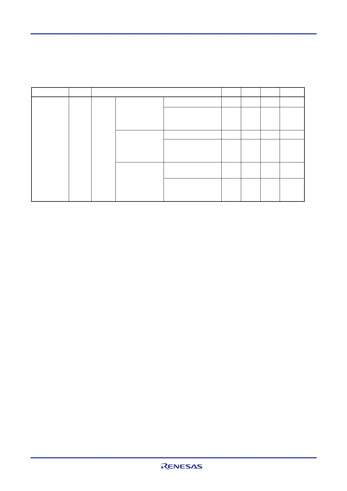
(6) Communication at different potential (2.5 V, 3 V) (UART mode) (dedicated baud rate generator output) (1/2)
(T
A = −40 to +85°C, 1.8 V ≤ EVDD0 = EVDD1 ≤ VDD ≤ 5.5 V, VSS = EVSS0 = EVSS1 = 0 V)
Parameter Symbol Conditions MIN. TYP. MAX. Unit
fMCK/6
Note 1
bps 4.0 V ≤ EVDD0 ≤ 5.5 V,
2.7 V ≤ V
b ≤ 4.0 V
Theoretical value of the
maximum transfer rate
f
CLK = 32 MHz, fMCK = fCLK
5.3 Mbps
fMCK/6
Note 1
bps 2.7 V ≤ EVDD0 < 4.0 V,
2.3 V ≤ V
b ≤ 2.7 V
Theoretical value of the
maximum transfer rate
f
CLK = 32 MHz, fMCK = fCLK
5.3 Mbps
f
MCK/6
Notes 1 to 3
bps
Transfer rate reception
1.8 V ≤ EV
DD0 < 3.3 V,
1.6 V ≤ V
b ≤ 2.0 V
Theoretical value of the
maximum transfer rate
f
CLK = 8 MHz, fMCK = fCLK
1.3 Mbps
Notes 1. Transfer rate in the SNOOZE mode : MAX. 9600 bps, MIN. 4800 bps
2. Use it with EV
DD0≥Vb.
3. The following conditions are required for low voltage interface when E
VDD0<VDD.
2.4 V ≤ EV
DD0 < 2.7 V : MAX. 2.6 Mbps
1.8 V ≤ EVDD0 < 2.4 V : MAX. 1.3 Mbps
1.6 V ≤ EV
DD0 < 1.8 V : MAX. 0.6 Mbps
Caution Select the TTL input buffer for the RxDq pin and the N-ch open drain output (V
DD tolerance) mode for
the TxDq pin by using port input mode register g (PIMg) and port output mode register g (POMg).
Remarks 1. V
b[V]: Communication line voltage
2. q: UART number (q = 0 to 3), g: PIM and POM number (g = 0, 1, 8, 14)
3. f
MCK: Serial array unit operation clock frequency
(Operation clock to be set by the CKSmn bit of serial mode register mn (SMRmn). m: Unit number,
n: Channel number (mn = 00 to 03, 10 to 13)
4. V
IH and VIL below are observation points for the AC characteristics of the serial array unit when
communicating at different potentials in UART mode.
4.0 V ≤ EV
DD0 ≤ 5.5 V, 2.7 V ≤ Vb ≤ 4.0 V: VIH = 2.2 V, VIL = 0.8 V
2.7 V ≤ EV
DD0 < 4.0 V, 2.3 V ≤ Vb ≤ 2.7 V: VIH = 2.0 V, VIL = 0.5 V
1.8 V ≤ EVDD0 < 3.3 V, 1.6 V ≤ Vb ≤ 2.0 V: VIH = 1.5 V, VIL = 0.32 V
5. UART2 cannnot communicate at different potential when bit 1 (PIOR1) of peripheral I/O redirection register
(PIOR) is 1.
<R>
<R>
<R>
<R>
<R>

 Loading...


