RL78/G13 CHAPTER 4 PORT FUNCTIONS
R01UH0146EJ0100 Rev.1.00 268
Sep 22, 2011
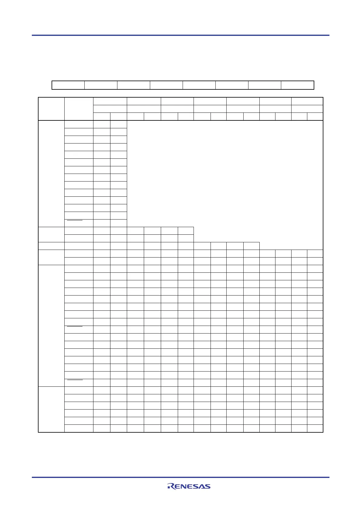
Figure 4-72. Format of Peripheral I/O Redirection Register (PIOR)
Address: F0077H After reset: 00H R/W
Symbol 7 6 5 4 3 2 1 0
PIOR 0 0 PIOR5 PIOR4 PIOR3 PIOR2 PIOR1 PIOR0
128/100-pin 80-pin 64-pin 52-pin 48-pin 44-pin
40/36/32/30
-pin
Setting value Setting value Setting value Setting value Setting value Setting value Setting value
Bit Function
0 1 0 1 0 1 0 1 0 1 0 1 0 1
INTP1 P46 P56
INTP3 P30 P57
INTP4 P31 P146
INTP6 P140 P84
INTP7 P141 P85
INTP8 P74 P86
INTP9 P75 P87
TxD1 P02 P82
RxD1 P03 P81
SCL10 P04 P80
SDA10 P03 P81
SI10 P03 P81
SO10 P02 P82
PIOR5
SCK10 P04 P80
This area cannot be used. Be set to 0 (default value).
PCLBUZ1 P141 P55 P141 P55 P141 P55PIOR4
INTP5 P16 P12 P16 P12 P16 P12
PIOR3 PCLBUZ0 P140 P31 P140 P31 P140 P31 P140 P31 P140 P31
SCLA0 P60 P14 P60 P14 P60 P14 P60 P14 P60 P14 P60 P14 P60 P14PIOR2
SDAA0 P61 P13 P61 P13 P61 P13 P61 P13 P61 P13 P61 P13 P61 P13
INTP10 P76 P110 P76 P110 P76 P52 P76 − − − − − − −
INTP11 P77 P111 P77 P111 P77 P53 P77 − − − − − − −
TxD2 P13 P77 P13 P77 P13 P77 P13 P77 P13 − P13 − P13 −
RxD2 P14 P76 P14 P76 P14 P76 P14 P76 P14 − P14 − P14 −
SCL20 P15 − P15 − P15 − P15 − P15 − P15 − P15 −
SDA20 P14 − P14 − P14 − P14 − P14 − P14 − P14 −
SI20 P14 − P14 − P14 − P14 − P14 − P14 − P14 −
SO20 P13 − P13 − P13 − P13 − P13 − P13 − P13 −
SCK20 P15 − P15 − P15 − P15 − P15 − P15 − P15 −
TxD0 P12 P17 P12 P17 P12 P17 P12 P17 P12 P17 P12 P17 P12 P17
RxD0 P11 P16 P11 P16 P11 P16 P11 P16 P11 P16 P11 P16 P11 P16
SCL00 P10 − P10 − P10 − P10 − P10 − P10 − P10 −
SDA00 P11 − P11 − P11 − P11 − P11 − P11 − P11 −
SI00 P11 P16 P11 P16 P11 P16 P11 − P11 − P11 − P11 −
SO00 P12 P17 P12 P17 P12 P17 P12 − P12 − P12 − P12 −
PIOR1
SCK00 P10 P55 P10 P55 P10 P55 P10 − P10 − P10 − P10 −
TI02/TO02 P17 P15 P17 P15 P17 P15 P17 P15 P17 P15 P17 P15 P17 P15
TI03/TO03 P31 P14 P31 P14 P31 P14 P31 P14 P31 P14 P31 P14 P31 P14
TI04/TO04 P42 P13 P42 P13 P42 P13 − P13 − P13 − P13 − P13
TI05/TO05 P46 P12 P05 P12 P05 P12 − P12 − P12 − P12 − P12
TI06/TO06 P102 P11 P06 P11 P06 P11 − P11 − P11 − P11 − P11
PIOR0
TI07/TO07 P145 P10 P41 P10 P41 P10 P41 P10 P41 P10 P41 P10 − P10
Cautions 1. If bit 1 (PIOR1) of the PIOR register is set to 1, the TxD2 and RxD2 pins are redirected, but SCL20,
SDA20, SI20, SO20, SCK20 pins are not redirected. Therefore, IIC20 and CSI20 cannot be used in
its setting. However, even if the bit is set to 1, CSI21/IIC21 can be used by P70 to P72 if UART2 is
not used.
2. For 20- to 25-pin products, PIOR register is not mounted.
<R>
<R>
 Loading...


