RL78/G13 CHAPTER 5 CLOCK GENERATOR
R01UH0146EJ0100 Rev.1.00 289
Sep 22, 2011
(2) System clock control register (CKC)
This register is used to select a CPU/peripheral hardware clock and a main system clock.
The CKC register can be set by a 1-bit or 8-bit memory manipulation instruction.
Reset signal generation sets this register to 00H.
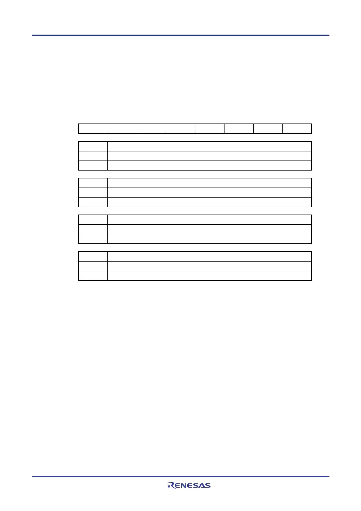
Figure 5-3. Format of System Clock Control Register (CKC)
Address: FFFA4H After reset: 00H R/W
Note 1
Symbol <7> <6> <5> <4> 3 2 1 0
CKC CLS CSS MCS MCM0 0 0 0 0
CLS Status of CPU/peripheral hardware clock (fCLK)
0 Main system clock (fMAIN)
1 Subsystem clock (fSUB)
CSS Selection of CPU/peripheral hardware clock (fCLK)
0 Main system clock (fMAIN)
1
Note 2
Subsystem clock (fSUB)
MCS Status of Main system clock (fMAIN)
0 High-speed on-chip oscillator clock (fIH)
1 High-speed system clock (fMX)
MCM0
Note 2
Main system clock (fMAIN) operation control
0 Selects the high-speed on-chip oscillator clock (fIH) as the main system clock (fMAIN)
1 Selects the high-speed system clock (fMX) as the main system clock (fMAIN)
Notes 1. Bits 7 and 5 are read-only.
2. Changing the value of the MCM0 bit is prohibited while the CSS bit is set to 1.
Remark f
IH: High-speed on-chip oscillator clock frequency
fMX: High-speed system clock frequency
f
MAIN: Main system clock frequency
f
SUB: Subsystem clock frequency
(Caution is listed on the next page.)
<R>

 Loading...


