RL78/G13 CHAPTER 5 CLOCK GENERATOR
R01UH0146EJ0100 Rev.1.00 303
Sep 22, 2011
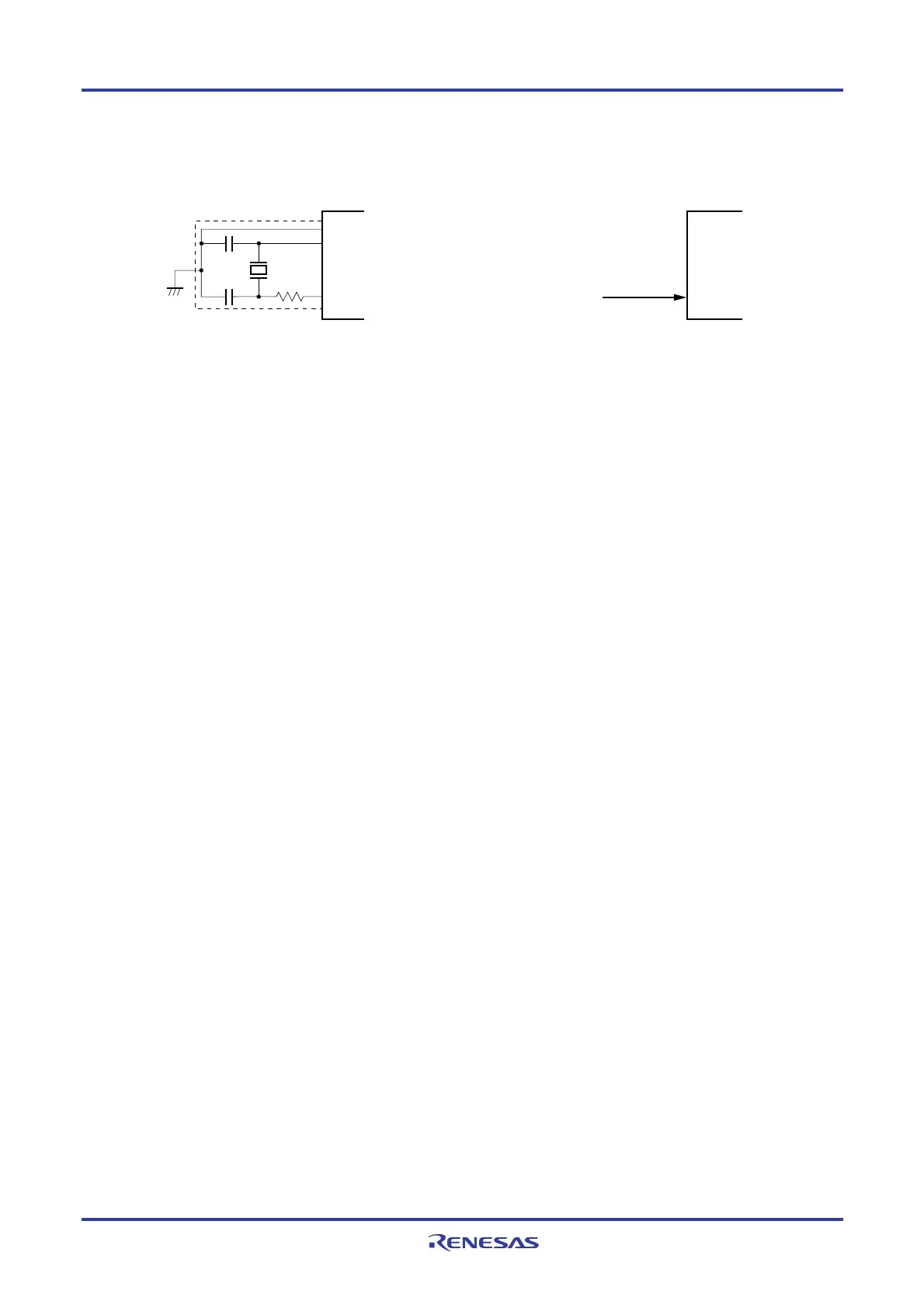
Figure 5-12. Example of External Circuit of XT1 Oscillator
(a) Crystal oscillation (b) External clock
XT2
V
SS
XT1
32.768
kHz
EXCLKS
External clock
Caution 1. When using the X1 oscillator and XT1 oscillator, wire as follows in the area enclosed by the
broken lines in the Figures 5-10 and 5-11 to avoid an adverse effect from wiring capacitance.
• Keep the wiring length as short as possible.
• Do not cross the wiring with the other signal lines. Do not route the wiring near a signal line
through which a high fluctuating current flows.
• Always make the ground point of the oscillator capacitor the same potential as V
SS. Do not
ground the capacitor to a ground pattern through which a high current flows.
• Do not fetch signals from the oscillator.
The XT1 oscillator is a circuit with low amplification in order to achieve low-power consumption.
Note the following points when designing the circuit.
• Pins and circuit boards include parasitic capacitance. Therefore, perform oscillation evaluation
using a circuit board to be actually used and confirm that there are no problems.
• When using the ultra-low power consumption oscillation (AMPHS1, AMPHS0 = 1, 0) as the mode
of the XT1 oscillator, use the recommended resonators described in CHAPTER 29 ELECTRICAL
SPECIFICATIONS.
• Make the wiring between the XT1 and XT2 pins and the resonators as short as possible, and
minimize the parasitic capacitance and wiring resistance. Note this particularly when the ultra-
low power consumption oscillation (AMPHS1, AMPHS0 = 1, 0) is selected.
• Configure the circuit of the circuit board, using material with little wiring resistance.
• Place a ground pattern that has the same potential as V
SS as much as possible near the XT1
oscillator.
• Be sure that the signal lines between the XT1 and XT2 pins, and the resonators do not cross
with the other signal lines. Do not route the wiring near a signal line through which a high
fluctuating current flows.
• The impedance between the XT1 and XT2 pins may drop and oscillation may be disturbed due
to moisture absorption of the circuit board in a high-humidity environment or dew
condensation on the board. When using the circuit board in such an environment, take
measures to damp-proof the circuit board, such as by coating.
• When coating the circuit board, use material that does not cause capacitance or leakage
between the XT1 and XT2 pins.

 Loading...


