RL78/G13 CHAPTER 25 FLASH MEMORY
R01UH0146EJ0100 Rev.1.00 931
Sep 22, 2011
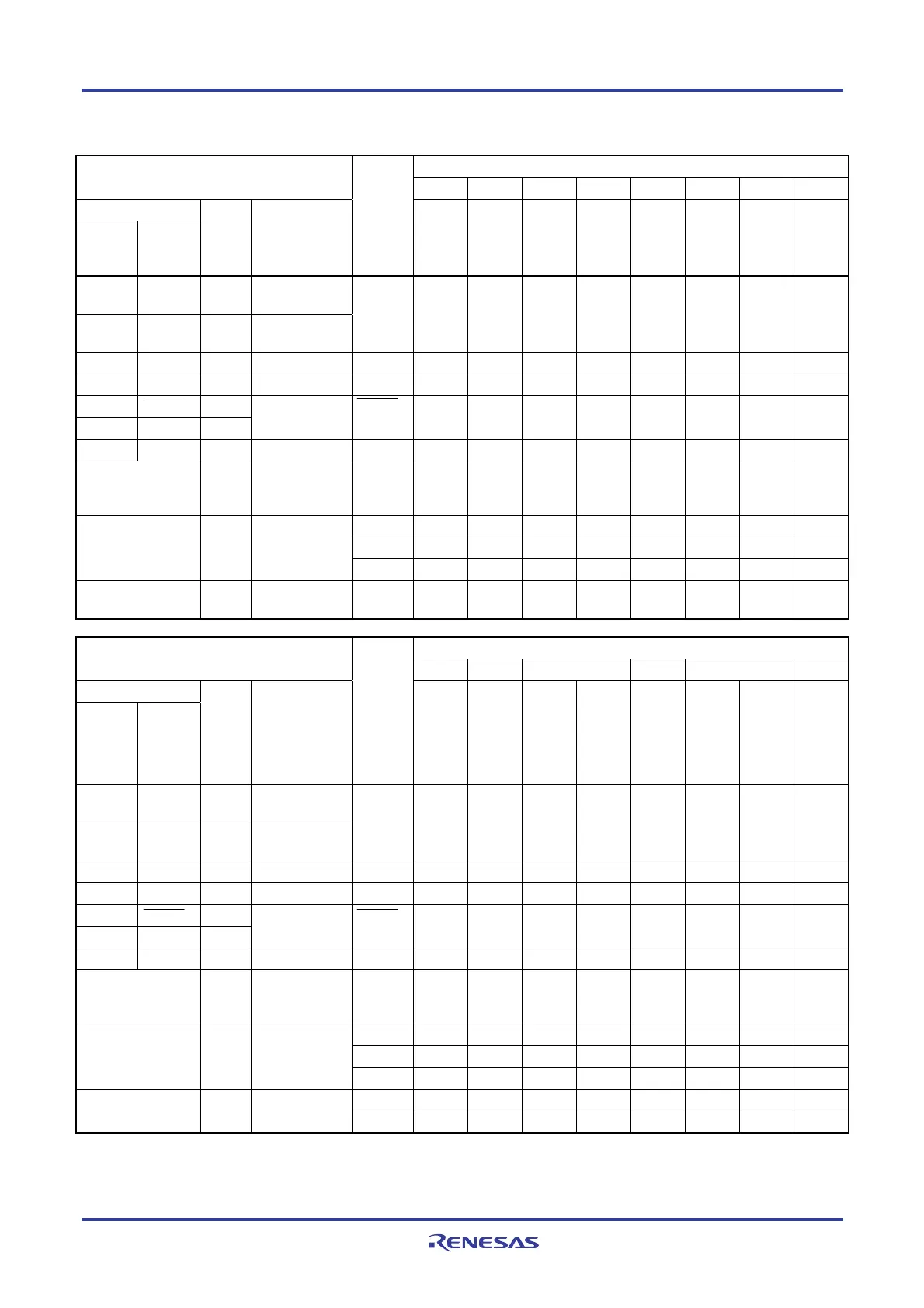
Table 25-1. Wiring Between RL78/G13 and Dedicated Flash Memory Programmer
Pin No.
Pin Configuration of Dedicated Flash Memory
Programmer
20-pin 24-pin 25-pin 30-pin 32-pin 36-pin 40-pin 44-pin
Signal Name
PG-FP5,
FL-PR5
E1 on-chip
debugging
emulator
I/O Pin Function
Pin Name
SSOP
WQFN
(4x4)
FLGA
(3x3)
SSOP
WQFN
(5x5)
FLGA
(4x4)
WQFN
(6x6)
LQFP
(10x10)
− TOOL0 I/O
Transmit/receiv
e signal
SI/RxD − I/O
Transmit/receiv
e signal
TOOL0/
P40
3 23 A5 5 1 6F 1 2
SCK − Output − − − − − − − − − −
CLK − Output − − − − − − − − − −
− RESET Output
/RESET − Output
Reset signal RESET 4 24 B5 6 2 5E 2 3
FLMD0 − Output Mode signal − − − − − − − − −
VDD I/O
V
DD voltage
generation/
power monitoring
V
DD 10 6 B3 12 8 6B 10 11
VSS 9 5 B2 11 7 5C 9 10
EVSS − − − − − − − −
GND − Ground
REGC
Note
8 4 A2 10 6 5D 8 9
EMVDD −
Driving power
for TOOL pin
V
DD 10 6 B3 12 8 6B 10 11
Pin No.
Pin Configuration of Dedicated Flash Memory
Programmer
48-pin 52-pin 64-pin 80-pin 100-pin 128-pin
Signal Name
PG-FP5,
FL-PR5
E1 on-chip
debugging
emulator
I/O Pin Function
Pin Name
LQFP
(7x7),
WQFN
(7x7)
LQFP
(10x10)
LQFP
(12x12),
LQFP
(10x10),
TQFP
(7x7)
FBGA
(4x4)
LQFP
(14x14),
LQFP
(12x12)
LQFP
(14x14)
LQFP
(14x20)
LQFP
(14x20)
− TOOL0 I/O
Transmit/receiv
e signal
SI/RxD − I/O
Transmit/receiv
e signal
TOOL0/
P40
39 4 5 D6 9 12 89 22
SCK − Output − − − − − − − − − −
CLK − Output − − − − − − − − − −
− RESET Output
/RESET − Output
Reset signal RESET 40 5 6 E7 10 13 90 26
FLMD0 − Output Mode signal − − − − − − − − −
VDD I/O
V
DD voltage
generation/
power monitoring
V
DD 48 13 15 B7 19 22 99 35
VSS 47 12 13 C7 17 20 97 33
EVSS − − 14 B8 18 21, 43 98, 20 34, 56
GND − Ground
REGC
Note
46 11 12 D7 16 19 96 32
VDD 48 13 − − − − − − EMVDD −
Driving power
for TOOL pin
EV
DD − − 16 A8 20 23, 53 100, 30 36, 57
Note Connect REGC pin to ground via a capacitor (default: 0.47
μ
F).
Remark Pins that are not indicated in the above table can be left open when using the flash memory programmer
for flash programming.
<R>

 Loading...


