Page 11 of 39 Rev. 13
2. MODBUS RTU
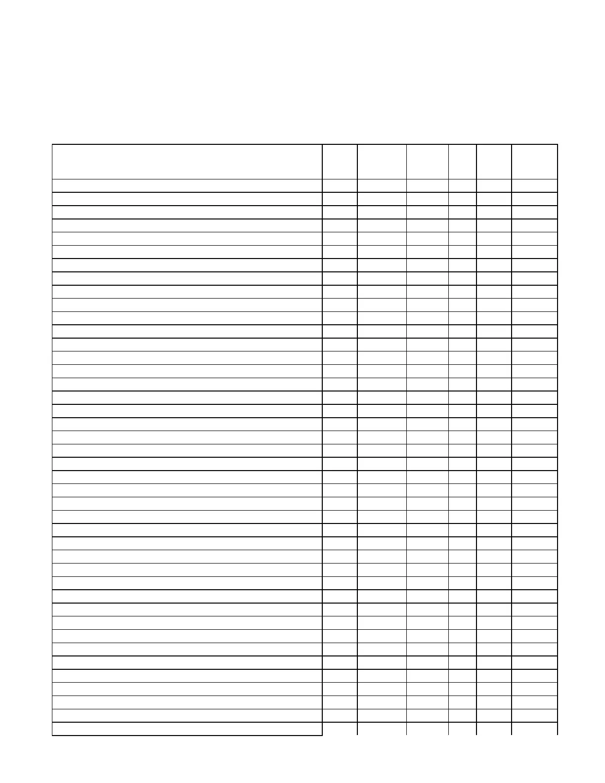
2.1 RAM MEMORY MAP
The following map shows the structure RAM of the PCOM card. (R) mean «readable » and (W) mean « writable ».
The function available is: Holding register (03), input register (04), write register (06), and preset multiple
register (16).
Variable
Unit
Address
(hex)
Addres
s (dec)
Byte
State
Note
Output voltage V 01 1 2 R note(1)
Output current A 02 2 2 R note(1)
Battery current A 03 3 2 R note(2)
AC volt phase 1 V 04 4 2 R note(1)
AC volt phase 2 V 05 5 2 R note(1)
AC volt phase 3 V 06 6 2 R note(1)
AC current phase 1 A 07 7 2 R note(1)
AC current phase 2 A 08 8 2 R note(1)
AC current phase 3 A 09 9 2 R note(1)
Battery temperature °C 0AH 10 1 R note(3)
Control board & inside temperature °C 0AL 10 1 R note(3)
AC frequency Hz 0B 11 2 R note(1)
Nominal output voltage V 0C 12 2 R note(1)
Nominal output current (Shunt1) A 0D 13 2 R note(1)
Float voltage V 0E 14 2 R/W note(1)
Equalize voltage V 0F 15 2 R/W note(1)
Float Current limit A 10 16 2 R/W note(1)
Equalize Current limit A 11 17 2 R/W note(1)
Formation voltage V 12 18 2 R/W note(1)
Formation current A 13 19 2 R/W note(1)
Formation relay 14H 20 1 R/W note(3)
Formation remaining time H 14L 20 1 R/W note(3)
Formation time H 15H 21 1 R/W note(3)
Charger state 15L 21 1 R note(8)
Charger configuration 16 22 2 R/W note(7)
Equalize mode start 17 23 2 R/W note(9)
Equalize remaining time out mn 18 24 2 R note(4)
Equalize elapsed time out mn 19 25 2 R note(4)
Manual equalize time out H 1AH 26 1 R/W note(3)
Periodical equalize time H 1AL 26 1 R/W note(3)
Periodical equalize period (delay) H 1BH 27 1 R/W note(3)
DC Low volts equalize time out H 1BL 27 1 R/W note(3)
DC Low volts equalize level V 1C 28 2 R/W note(1)
AC fail equalize time out H 1DH 29 1 R/W note(3)
AC fail equalize delay S 1DL 29 1 R/W note(3)
Refresh equalize time out mn 1EH 30 1 R/W note(3)
Refresh equalize period (delay) H 1EL 30 1 R/W note(3)
Remote equalize time out H 1F H 31 1 R/W note(3)
Current limit equalize time out H 1FL 31 1 R/W note(3)
Current limit equalize delay S 20H 32 1 R/W note(3)
Equalize termination (On/Off) 20L 32 1 R/W note(10)
Post Charge Voltage delay mn 21 33 2 R/W note(4)
 Loading...