MIPI CSI-2 RX Subsystem v4.0 34
PG232 July 02, 2019 www.xilinx.com
Chapter 2: Product Specification
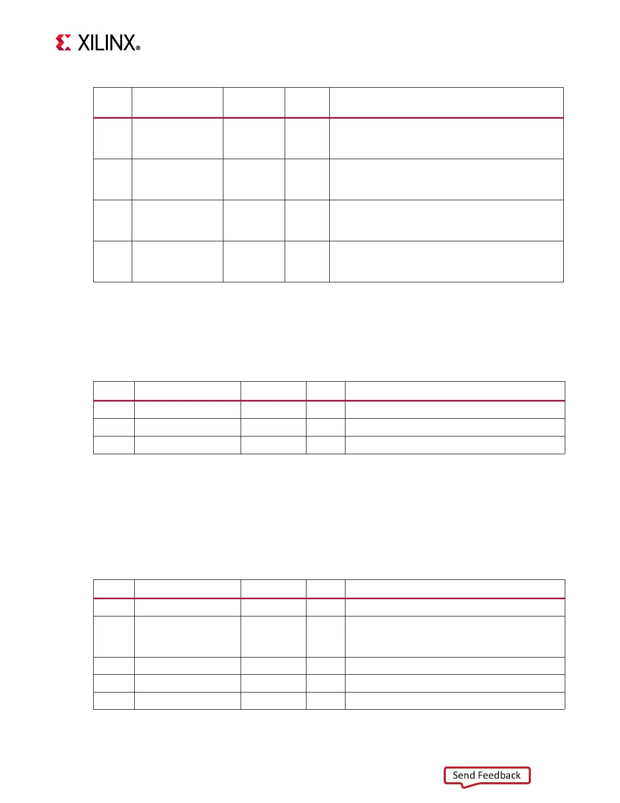
Clock Lane Information Register
The Clock Lane Information register is described in Tab l e 2 - 28. The Stop state is captured in
this register.
Lane<n> Information Registers
The Lane<n> Information register, where n is 0, 1, 2 or 3, is described in Tabl e 2- 2 9 and
provides the status of the <n> data lane. This register is reset when any write to the
Protocol Configuration register is detected, irrespective of whether the Protocol
Configuration register contents are updated or not.
3Frame
synchronization
error for VC5
R/W1C 0x0 Asserted when an FE is not paired with a Frame
Start (FS) on the same virtual channel.
2 Frame level error
for VC5
R/W1C 0x0 Asserted after an FE when the data payload
received between FS and FE contains errors. The
data payload errors are CRC errors.
1Frame
synchronization
error for VC4
R/W1C 0x0 Asserted when an FE is not paired with a Frame
Start (FS) on the same virtual channel.
0 Frame level error
for VC4
R/W1C 0x0 Asserted after an FE when the data payload
received between FS and FE contains errors. The
data payload errors are CRC errors.
Table 2-28: Clock Lane Information Register (0x3C)
Bits Name Reset Value Access Description
31–2 Reserved N/A N/A Reserved
1 Stop state 0x0 R Stop state on clock lane
0 Reserved N/A N/A Reserved
Table 2-29: Lane 0, 1, 2, 3 Information Register (0x40, 0x44, 0x48, 0x4C)
Bits Name Reset Value Access Description
(2)
31–6 Reserved N/A N/A Reserved
5Stop state 0x0 R
Detection of Stop state
Active-High signal indicates that the lane
module is currently in stop state
4 Reserved N/A N/A Reserved
3 Reserved N/A N/A Reserved
2 Reserved N/A N/A Reserved
Table 2-27: VCX Frame Error (0x34) (Cont’d)
Bits Name Access
Default
Value
Description
 Loading...