MIPI CSI-2 RX Subsystem v4.0 35
PG232 July 02, 2019 www.xilinx.com
Chapter 2: Product Specification
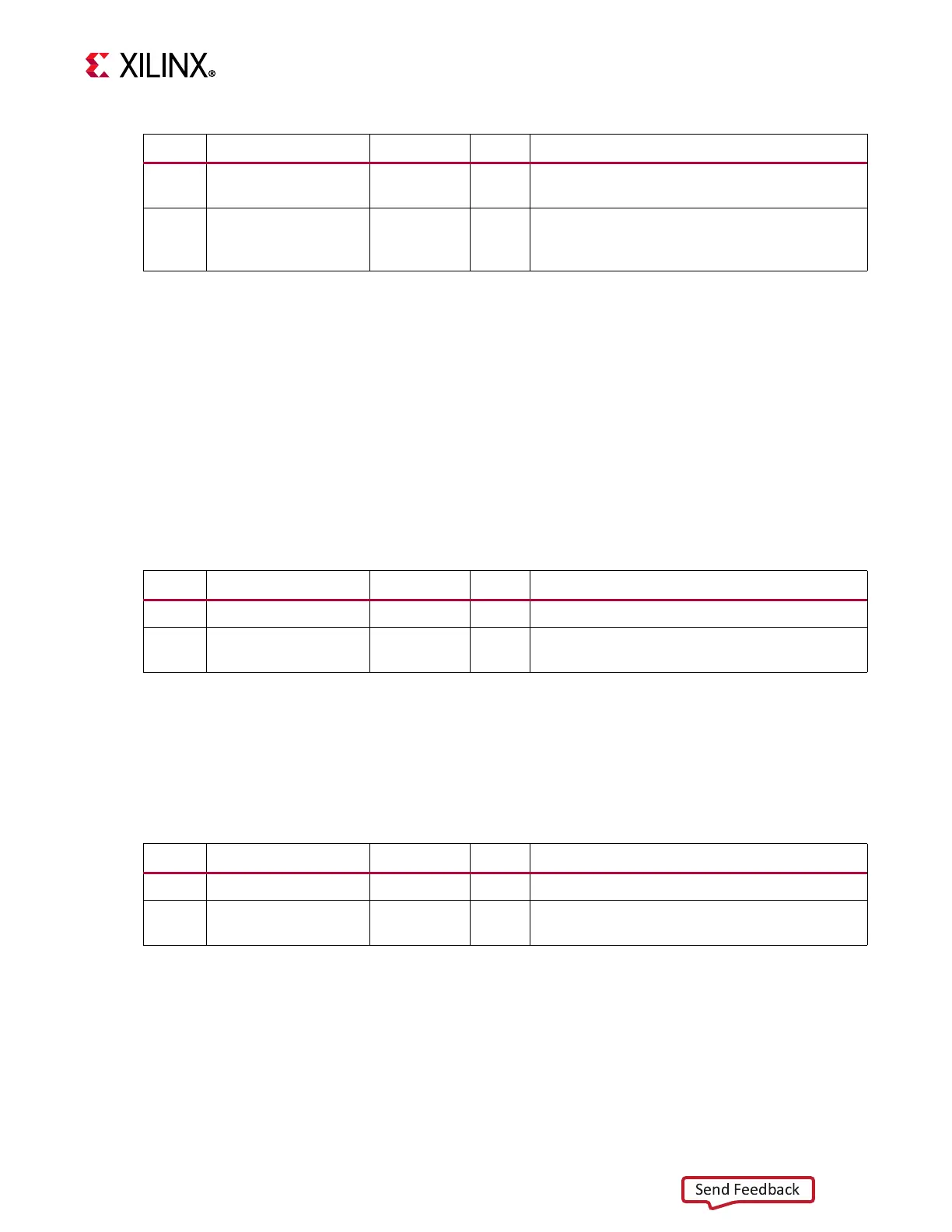
Image Information 1 Registers (VC0 to VC15)
The Image Information 1 registers are described in Ta b le 2 - 3 0 and provide image
information for line count and byte count per VC. The byte count gets updated whenever a
long packet (from Data Types 0x18 and above) for the corresponding virtual channel is
processed by the control FSM. The line count is updated whenever the packet is written into
the line buffer.
Image Information 2 Registers (VC0 to VC15)
The Image Information 2 registers are described in Ta b le 2 - 3 1 and provide the image
information Data Type. The Data Type is updated whenever a long packet (Data Types 0x18
and above) for the corresponding virtual channel is processed by the control FSM.
AXI IIC Registers
The AXI IIC registers are available when Include IIC is selected in the Vivado IDE. For details
about AXI IIC registers, see the AXI IIC Bus Interface v2.0 LogiCORE IP Product Guide (PG090)
[Ref 5].
1 SoT error 0x0 R
Detection of SoT Error (ErrSotHS)
Indicates SoT error detected
0 SoT Sync error 0x0 R
Detection of SoT Synchronization Error
(ErrSotSyncHS)
Indicates that SoT synchronization failed
Notes:
1. Lane Information registers are present only for the maximum defined number of lanes. Reads to others registers
gives 0x0.
2. All bits are reported through the PPI.
Table 2-30: Image Information 1 Registers (0x60, 0x68, 0x70, 0x78)
Bits Name Reset Value Access Description
31–16 Line count 0x0 R Number of long packets written to line buffer
15–0 Byte count 0x0 R
Byte count of current packet being processed
by the control FSM
Table 2-31: Image Information 2 Registers (0x64, 0x6C, 0x74, 0x7C)
Bits Name Reset Value Access Description
31–6 Reserved N/A N/A Reserved
5–0 Data Type 0x0 R
Dat a Type of cur r ent packe t being pr o cessed by
control FSM
Table 2-29: Lane 0, 1, 2, 3 Information Register (0x40, 0x44, 0x48, 0x4C) (Cont’d)
Bits Name Reset Value Access Description
(2)
 Loading...