MIPI CSI-2 RX Subsystem v4.0 57
PG232 July 02, 2019 www.xilinx.com
Chapter 4: Design Flow Steps
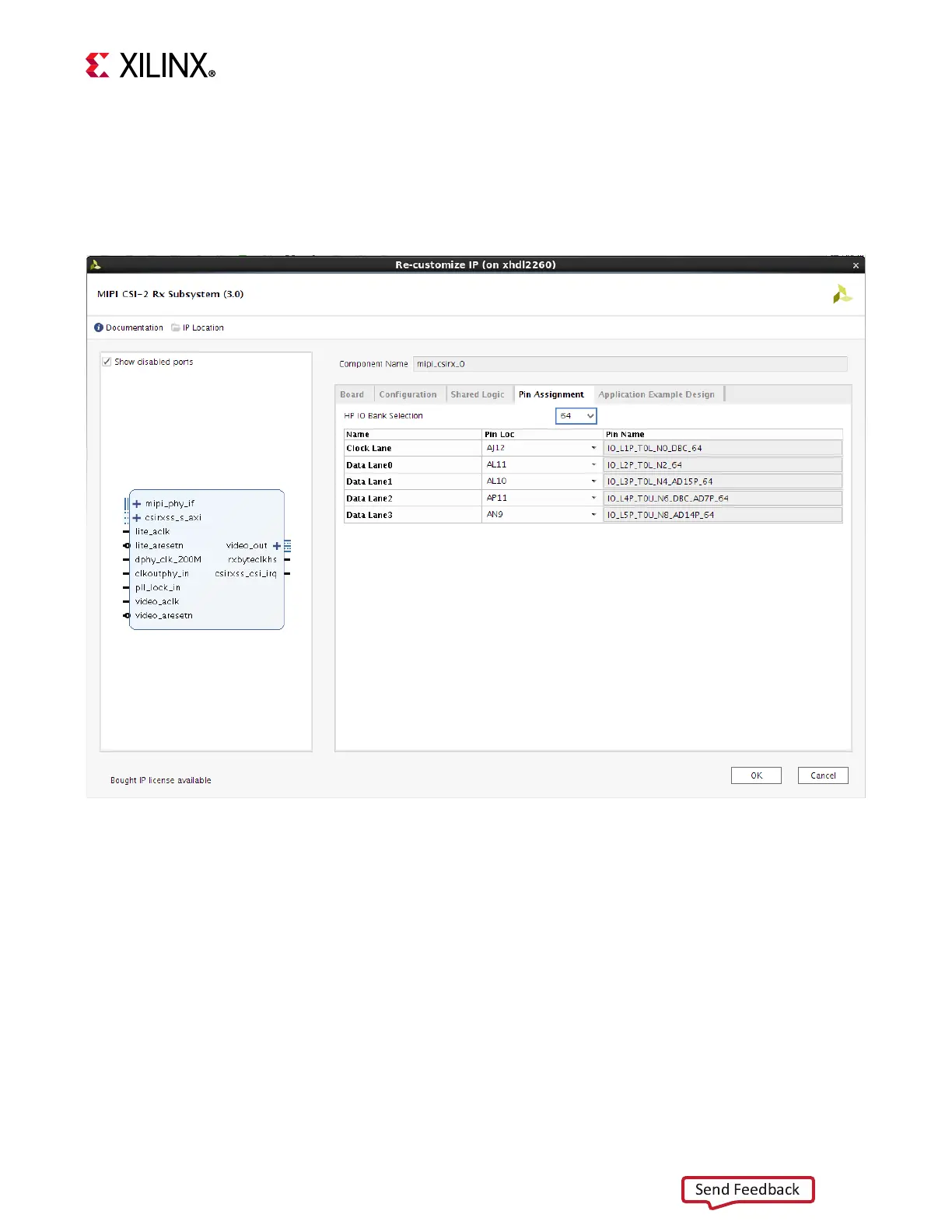
Pin Assignment Tab
The Pin Assignment tab page allows to select pins. The subsystem pin assignment
configuration screen is shown in Figure 4-4.
Note:
This tab is not available for Xilinx 7 Series device configurations.
HP IO Bank Selection: Select the HP I/O bank for clock lane and data lane implementation.
Clock Lane: Select the LOC for clock lane. This selection determines the I/O byte group
within the selected HP I/O bank.
Data Lane 0/1/2/3: Displays the Data lanes 0, 1, 2, and 3 LOC based on the clock lane
selection.
Application Example Design
The Application Example Design tab page provides example design parameters. The
subsystem application example design configuration screen is shown in Figure 4-5.
X-Ref Target - Figure 4-4
Figure 4-4: Subsystem Customization Screen - Pin Assignment
 Loading...