MIPI CSI-2 RX Subsystem v4.0 17
PG232 July 02, 2019 www.xilinx.com
Chapter 2: Product Specification
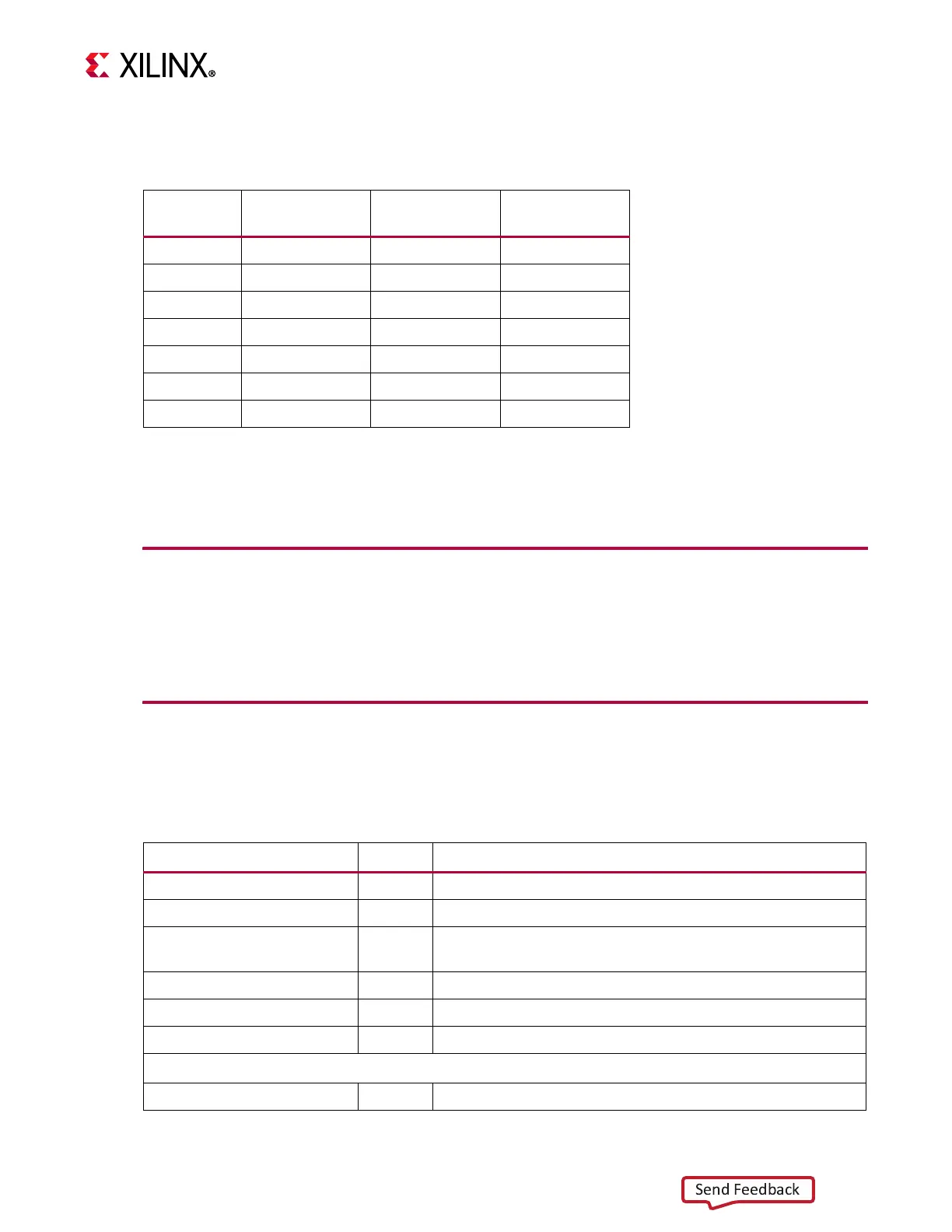
Tab l e 2 - 4 provides the overall latency numbers of MIPI CSI2 RX Subsystem for various core
configurations.
Resource Utilization
For full details about performance and resource utilization, visit the Performance and
Resource Utilization web page.
Port Descriptions
The MIPI CSI-2 RX Subsystem I/O signals are described in Ta b le 2-5.
Table 2-4: MIPI CSI2 RX Subsystem Latency
Data Type Pixel Mode Line Rate
Latency in
rxbyteclk
RAW20 Single
1000 61
RAW8 Single
1000 48
RAW8 Dual
1000 48
RAW8 Quad
1000 48
RAW10 Single
1000 53
RAW10 Dual
1200 59
RAW10 Quad
800 47
Notes:
1. All the calculations are made for a single lane design with a fixed video
clock of 148 MHz.
2. The latency is improved by increasing the number of lanes.
Table 2-5: Port Descriptions
Signal Name Direction Description
lite_aclk Input AXI clock
lite_aresetn Input AXI reset. Active-Low
S00_AXI*
AXI4-Lite interface, defined in the Vivado Design Suite: AXI
Reference Guide (UG1037) [Ref 7]
dphy_clk_200M Input Clock for D-PHY core. Must be 200 MHz.
video_aclk Input Subsystem clock
video_aresetn
(1)
Input Subsystem reset. Active-Low.
AXI4-Stream Video Interface when Video Format Bridge is Present
video_out_tvalid Output Data valid
 Loading...