ZCU106 Board User Guide 81
UG1244 (v1.0) March 28, 2018 www.xilinx.com
Chapter 3: Board Component Descriptions
SFP/SFP+ Clock Recovery
[Figure 2-1, callout 11]
The ZCU106 board includes a Silicon Labs Si5328B jitter attenuator U20 (8 kHz – 808 MHz).
The FPGA can output the RX recovered clock to a differential I/O pair on I/O bank 68
(SFP_REC_CLOCK_C_P, pin H11 and SFP_REC_CLOCK_C_N, pin G11) for jitter attenuation. The
jitter attenuated clock (SFP_SI5328_OUT_C_P (U20 pin 28), SFP_SI5328_OUT_C_N (U20 pin
29)) is then routed as a series capacitor coupled reference clock to GTH Quad 225 inputs
MGTREFCLK1P (U1 pin W10) and MGTREFCLK1N (U1 pin W9).
The primary purpose of this clock is to support synchronous protocols such as CPRI or
OBSAI to perform clock recovery from a user-supplied SFP/SFP+ module and use the jitter
attenuated recovered clock to drive the reference clock inputs of a GTH transceiver. The
system controller configures the SI5328B in free-run mode (see TI MSP430 System
Controller, page 116). The jitter attenuated clock circuit is shown in Figure 3-30.
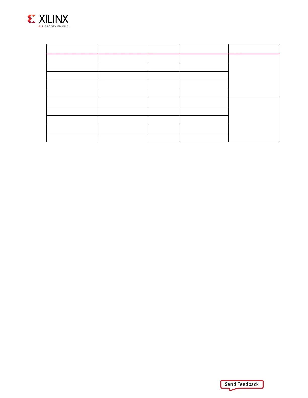
Table 3-32: ZCU106 FPGA U1 to SFP0 and SFP1 Module Connections
XCZU7EV (U1) Pin Net Name Pin No. Pin Name SFP/SFP+ Module
Y4 SFP0_TX_P 18 TD_P
P1
Y3 SFP0_TX_N 19 TD_N
AA2 SFP0_RX_P 13 RD_P
AA1 SFP0_RX_N 12 RD_N
AE22 SFP0_TX_DISABLE_B 3 TX_DISABLE
W6 SFP1_TX_P 18 TD_P
P2
W5 SFP1_TX_N 19 TD_N
W2 SFP1_RX_P 13 RD_P
W1 SFP1_RX_N 12 RD_N
AF20 SFP1_TX_DISABLE_B 3 TX_DISABLE
Notes:
1. SFPx_TX_DISABLE_B nets implement the LVCMOS33 standard.