ZCU106 Board User Guide 100
UG1244 (v1.0) March 28, 2018 www.xilinx.com
Chapter 3: Board Component Descriptions
PCI Express Endpoint Connectivity
[Figure 2-1, callout 36]
The 4-lane PCI Express edge connector P3 performs data transfers at the rate of 2.5 GT/s for
Gen1 applications, 5.0 GT/s for Gen2 applications, and 8.0 GT/s for Gen3 applications. The
PCIe transmit and receive signal data paths have a characteristic impedance of 85Ω ±10%.
The PCIe clock is routed as a 100Ω differential pair. The XCZU7EV (-2 speed grade) supports
up to Gen3 x8.
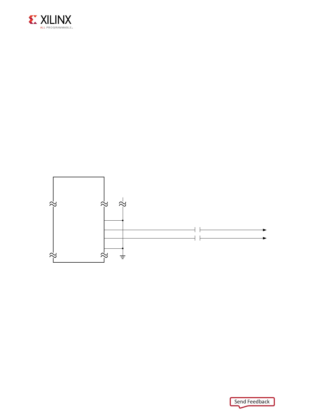
The PCIe reference clock input is from the P3 edge connector. It is AC coupled to MPSoC U1
through the MGTREFCLK0 pins of Quad 224. PCIE_CLK_P is connected to U1 pin AB8, and
the _N net is connected to pin AB7. The PCI Express clock connection is shown in
Figure 3-39 and the PCI Express connector is shown in Figure 3-40.
PCIe lane size is selected by jumper J162 as shown in Figure 3-40. The default lane size
selection is 4-lane (J162 pins 2 and 4 jumped).
X-Ref Target - Figure 3-39
Figure 3-39: PCIe Edge Connector Clock
PCI Express
Four-Lane
Edge Connector
OE
GND
REFCLK+
REFCLK-
GND
A12
A13
A14
A15
PCIE_CLK_Q0_C_P
PCIE_CLK_Q0_C_N
GND
PCIE_CLK_Q0_P
PCIE_CLK_Q0_N
C340
0.1 μf
0.1 μf
C339
P3
X19199-050117