ZCU106 Board User Guide 33
UG1244 (v1.0) March 28, 2018 www.xilinx.com
Chapter 3: Board Component Descriptions
The ZCU106 DDR4 SODIMM interface adheres to the constraints guidelines documented in
the “PCB Guidelines for DDR4” section of the UltraScale Architecture PCB Design Guide
(UG583) [Ref 3]. The DDR4 SODIMM interface is a 40Ω impedance implementation. Other
memory interface details are also available in the UltraScale Architecture FPGAs Memory
Interface Solutions Guide (PG150) [Ref 4].
DDR4 Component Memory
[Figure 2-1, callout 2]
The 2 GB 64-bit wide DDR4 memory system is comprised of four 256 Mb x 16 SDRAMs
(Micron MT40A256M16GE-075E) U2 and 99–101. This memory system is connected to
PL-side XCZU7EV banks 64, 65, and 66. The DDR4 0.6V VTT termination voltage is supplied
from sink-source regulator U35. The connections between the DDR4 memory and the
XCZU7EV device are listed in Table 3-4.
AP33 DDR4_SODIMM_CS0_B 149 CS0_N
AK32 DDR4_SODIMM_CS1_B 157 CS1_N
Table 3-3: DDR4 SODIMM Socket J1 Connections to FPGA PS DDR Bank 504 (Cont’d)
XCZU7EV (U1) Pin Net Name
DDR4 SODIMM Memory J1
Pin Number Pin Name
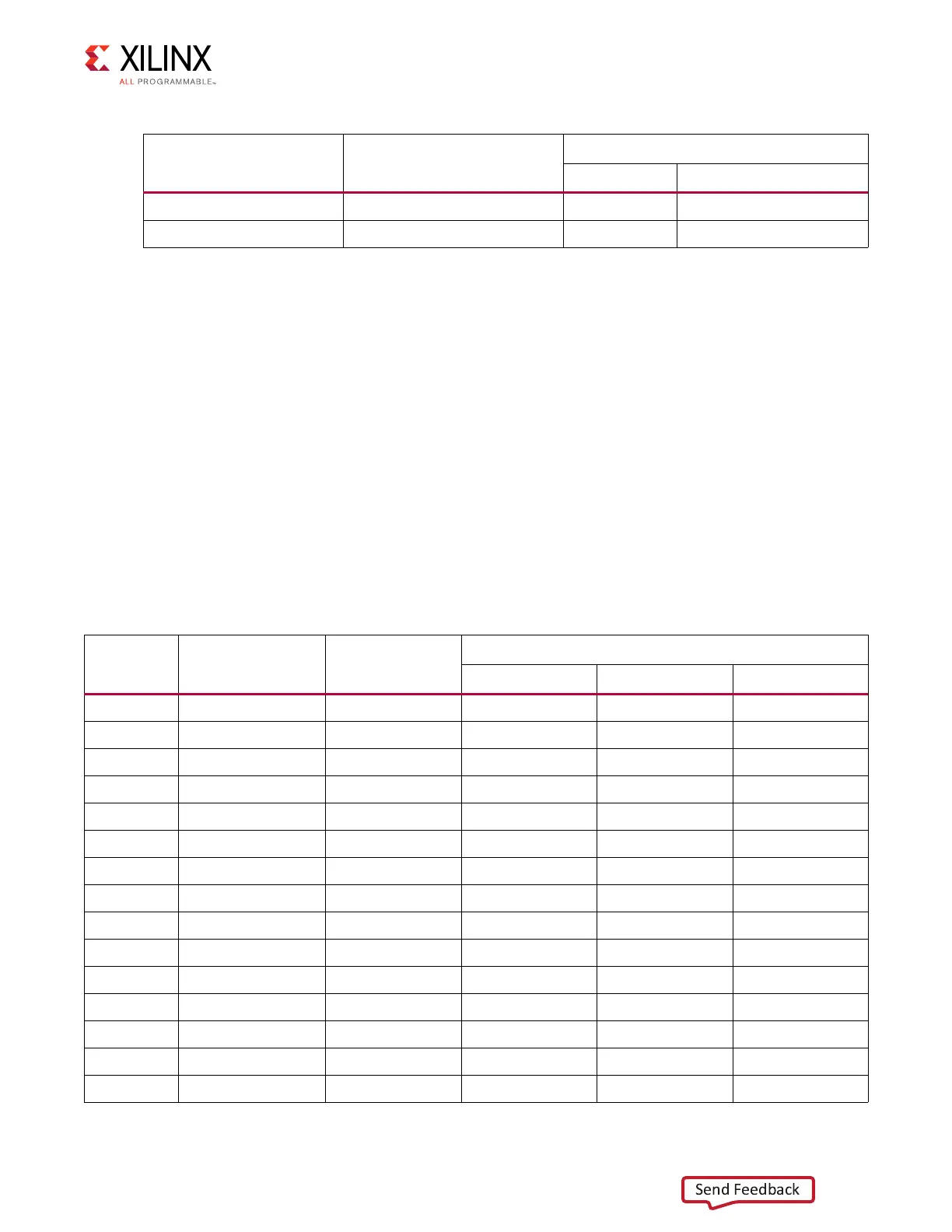
Table 3-4: DDR4 Component Memory Connection to the XCZU7EV MPSoC
XCZU7EV
(U1) Pin
Net Name I/O Standard
DDR4 Component Memory
Pin # Pin Name Ref. Des.
AF16 DDR4_DQ0 POD12_DCI G2 DQL0 U101
AF18 DDR4_DQ1 POD12_DCI F7 DQL1 U101
AG15 DDR4_DQ2 POD12_DCI H3 DQL2 U101
AF17 DDR4_DQ3 POD12_DCI H7 DQL3 U101
AF15 DDR4_DQ4 POD12_DCI H2 DQL4 U101
AG18 DDR4_DQ5 POD12_DCI H8 DQL5 U101
AG14 DDR4_DQ6 POD12_DCI J3 DQL6 U101
AE17 DDR4_DQ7 POD12_DCI J7 DQL7 U101
AA14 DDR4_DQ8 POD12_DCI A3 DQU0 U101
AC16 DDR4_DQ9 POD12_DCI B8 DQU1 U101
AB15 DDR4_DQ10 POD12_DCI C3 DQU2 U101
AD16 DDR4_DQ11 POD12_DCI C7 DQU3 U101
AB16 DDR4_DQ12 POD12_DCI C2 DQU4 U101
AC17 DDR4_DQ13 POD12_DCI C8 DQU5 U101
AB14 DDR4_DQ14 POD12_DCI D3 DQU6 U101