ZCU106 Board User Guide 28
UG1244 (v1.0) March 28, 2018 www.xilinx.com
Chapter 3: Board Component Descriptions
I/O Voltage Rails
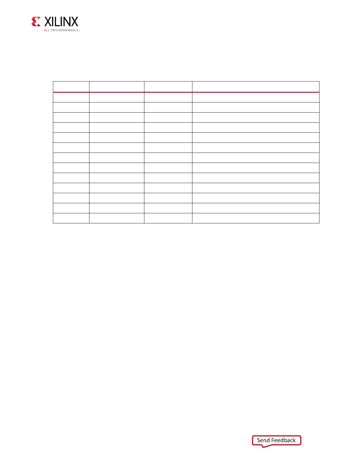
The XCZU7EV MPSoC PL I/O bank voltages on the ZCU106 board are listed in Figure 3-2.
PS-Side: DDR4 SODIMM Socket
[Figure 2-1, callout 2]
The PS-side memory is wired to the Zynq UltraScale+ DDRC bank 504 hard memory
controller. A 64-bit single rank DDR4 SODIMM with ECC (72-bit) is inserted into socket J1.
The ZCU106 is shipped with a DDR4 SODIMM installed:
• Manufacturer: Kingston
• Part Number: KVR21SE15S8/4
•Description:
°
4 GByte DDR4 SODIMM
°
Single rank x8
°
512 Mbit x 72-Bit
°
PC4-2133 260-Pin
Table 3-2: I/O Voltage Rails
XCZU7EV Power Net Name Voltage Connected To
PL Bank 28 V
ADJ_FMC
(1)
1.8V FMC_HPC1 LA BUS, PMOD0
PL Bank 64 V
CC1V2
1.2V DDR4 DQ[0:31]
PL Bank 65 V
CC1V2
1.2V DDR4 DQ[32:63]
PL Bank 66 V
CC1V2
1.2V DDR4 ADDR/CTRL, GPIO LED, GPIO SW, PMOD1
PL Bank 67 V
ADJ_FMC
(1)
1.8V FMC_HPC0 LA BUS, GPIO DIP SW
PL Bank 68 V
ADJ_FMC
(1)
1.8V FMC_HPC0 LA BUS, SFP REC CLOCK
PL Bank 87 V
CC3V3
3.3V HDMI, MSP430 GPIO
PL Bank 88 V
CC3V3
3.3V TRACE DEBUG CONNECTOR
PS Bank 500 V
CCOPS
1.8V CAN, UART0/1, I2C0/1, QSPI LWR/UPR
PS Bank 501 V
CCOPS
1.8V SDIO, PMU_GPO[0:5], DP
PS Bank 502 V
CCOPS
1.8V ENET, USB_DATA[0:7], USB_CTRL
PS Bank 503 V
CCOPS3
1.8V PS CONFIG I/F
PS Bank 504 V
CCO_PSDDR_504
1.2V DDR4 72-BIT SODIMM I/F
Notes:
1. The ZCU106 board is shipped with V
ADJ_FMC
set to 1.8V by the MSP430 system controller.