Service Guide E8361-90001 5-23
PNA Series Microwave Network Analyzers Theory of Operation
E8361A Frequency Offset Group Operation (Option 080)
Frequency Offset Group Operation (Option 080)
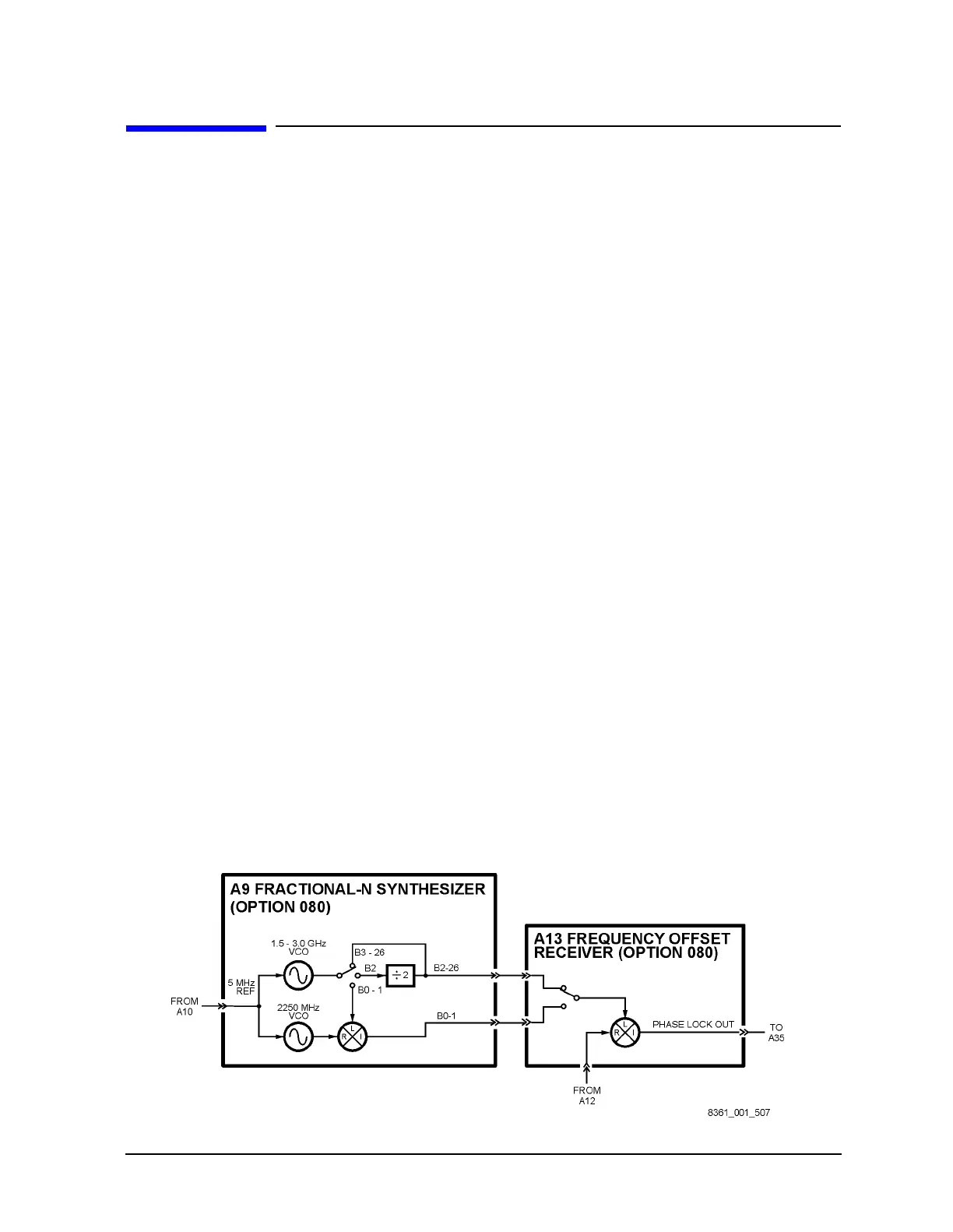
The frequency offset group provides the circuitry necessary to phase lock the analyzer
while the source and receiver are tuned to different frequencies. Figure 5-7 on page 5-23 is
a simplified block diagram of the frequency offset functional group.
In this section the following assemblies are described:
• A9 Fractional-N Synthesizer Board
• A13 Frequency Offset Receiver Assembly
A9 Fractional-N Synthesizer Board
The A9 fractional-N synthesizer is identical to the A8 fractional-N synthesizer. Therefore,
the values listed in Table 5-2 on page 5-8 for the A8, apply to both the A8 and A9.
The A9 fractional-N synthesizer board uses the 5 MHz reference signal from the A10
frequency reference board to tune two VCO circuits: one that sweeps from 1500 to
3010 MHz and one that is set to a CW frequency of 2250 MHz. In bands 0–1, these two
signals are heterodyned to produce the output frequencies listed in Table 5-2 on page 5-8.
In band 2, the output of the swept VCO is passed through a divide-by-2 circuit to produce
the output frequencies listed in Table 5-2. In all other bands, the swept VCO signal is sent
directly to the synthesizer output.
At the output, an ALC circuit maintains the power level at −5 dBm ± 2 dB for bands 0–2 or
−1.5 dBm ± 1.5dB for bands 3–26. In all bands, the output is sent to the A13 frequency
offset receiver assembly.
A13 Frequency Offset Receiver Assembly
The A13 frequency offset receiver assembly consists of a frequency offset receiver board
and a separate receiver module.
The output of the A9 fractional-N synthesizer board is directed to the receiver module
where it is mixed with a signal from the A12 source assembly to produce a phase lock
output signal.
This phase lock signal is sent to a multiplexer on the A35 receiver motherboard, the output
of which is routed to the A11 phase lock board to complete the phase lock loop. Refer to
“Phase Lock Control” on page 5-22.
Figure 5-7 Frequency Offset Group
 Loading...