130
2467S–AVR–07/09
ATmega128
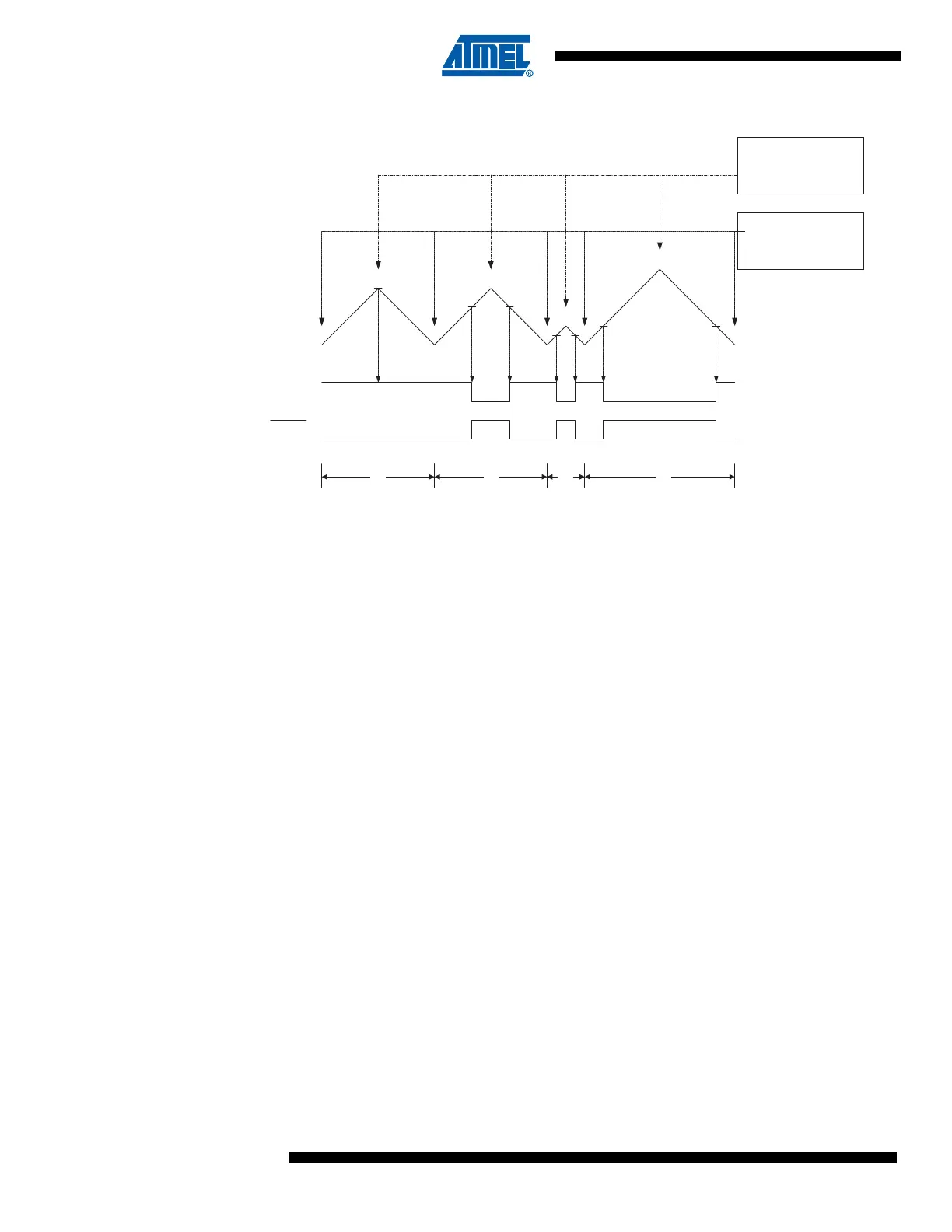
Figure 54. Phase and Frequency Correct PWM Mode, Timing Diagram
The Timer/Counter Overflow Flag (TOVn) is set at the same timer clock cycle as the OCRnx
Registers are updated with the double buffer value (at BOTTOM). When either OCRnA or ICRn
is used for defining the TOP value, the OCnA or ICFn flag set when TCNTn has reached TOP.
The interrupt flags can then be used to generate an interrupt each time the counter reaches the
TOP or BOTTOM value.
When changing the TOP value the program must ensure that the new TOP value is higher or
equal to the value of all of the compare registers. If the TOP value is lower than any of the com-
pare registers, a compare match will never occur between the TCNTn and the OCRnx.
As Figure 54 shows the output generated is, in contrast to the phase correct mode, symmetrical
in all periods. Since the OCRnx Registers are updated at BOTTOM, the length of the rising and
the falling slopes will always be equal. This gives symmetrical output pulses and is therefore fre-
quency correct.
Using the ICRn Register for defining TOP works well when using fixed TOP values. By using
ICRn, the OCRnA Register is free to be used for generating a PWM output on OCnA. However,
if the base PWM frequency is actively changed by changing the TOP value, using the OCRnA as
TOP is clearly a better choice due to its double buffer feature.
In phase and frequency correct PWM mode, the compare units allow generation of PWM
waveforms on the OCnx pins. Setting the COMnx1:0 bits to 2 will produce a non-inverted PWM
and an inverted PWM output can be generated by setting the COMnx1:0 to 3 (See Table 60 on
page 134). The actual OCnx value will only be visible on the port pin if the data direction for the
port pin is set as output (DDR_OCnx). The PWM waveform is generated by setting (or clearing)
the OCnx Register at the compare match between OCRnx and TCNTn when the counter
increments, and clearing (or setting) the OCnx Register at compare match between OCRnx and
TCNTn when the counter decrements. The PWM frequency for the output when using phase
and frequency correct PWM can be calculated by the following equation:
The N variable represents the prescaler divider (1, 8, 64, 256, or 1024).
OCRnx / TOP Update
and
TOVn Interrupt Flag Set
(Interrupt on Bottom)
OCnA Interrupt Flag Set
or ICFn Interrupt Flag Set
(Interrupt on TOP)
1 2 3 4
TCNTn
Period
OCnx
OCnx
(COMnx1:0 = 2)
(COMnx1:0 = 3)
f
OCnxPFCPWM
f
clk_I/O
2 NTOP⋅⋅
----------------------------=