256
2467S–AVR–07/09
ATmega128
Scanning the Digital
Port Pins
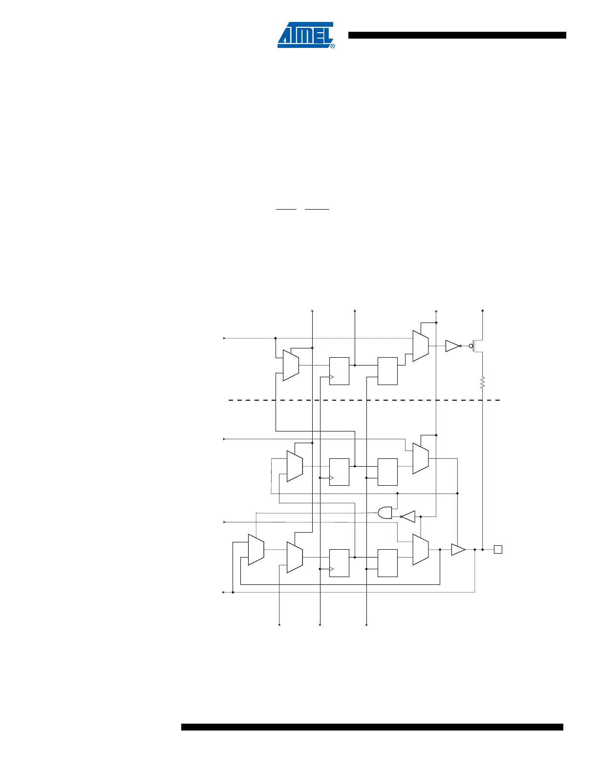
Figure 124 shows the Boundary-scan Cell for a bi-directional port pin with pull-up function. The
cell consists of a standard Boundary-scan cell for the Pull-up Enable – PUExn – function, and a
bi-directional pin cell that combines the three signals Output Control – OCxn, Output Data –
ODxn, and Input Data – IDxn, into only a two-stage Shift Register. The port and pin indexes are
not used in the following description
The Boundary-scan logic is not included in the figures in the Data Sheet. Figure 125 shows a
simple digital Port Pin as described in the section “I/O Ports” on page 66. The Boundary-scan
details from Figure 124 replaces the dashed box in Figure 125.
When no alternate port function is present, the Input Data – ID corresponds to the PINxn Regis-
ter value (but ID has no synchronizer), Output Data corresponds to the PORT Register, Output
Control corresponds to the Data Direction – DD Register, and the Pull-up Enable – PUExn – cor-
responds to logic expression PUD
· DDxn · PORTxn.
Digital alternate port functions are connected outside the dotted box in Figure 125 to make the
scan chain read the actual pin value. For Analog function, there is a direct connection from the
external pin to the analog circuit, and a scan chain is inserted on the interface between the digi-
tal logic and the analog circuitry.
Figure 124. Boundary-scan Cell for Bi-directional Port Pin with Pull-Up Function.
DQ DQ
G
0
1
0
1
DQ DQ
G
0
1
0
1
0
1
0
1
DQ DQ
G
0
1
Port Pin (PXn)
VccEXTESTTo Next CellShiftDR
Output Control (OC)
Pullup Enable (PUE)
Output Data (OD)
Input Data (ID)
From Last Cell
UpdateDRClockDR
FF2 LD2
FF1 LD1
LD0FF0