128
7647H–AVR–03/12
Atmel ATmega16/32/64/M1/C1
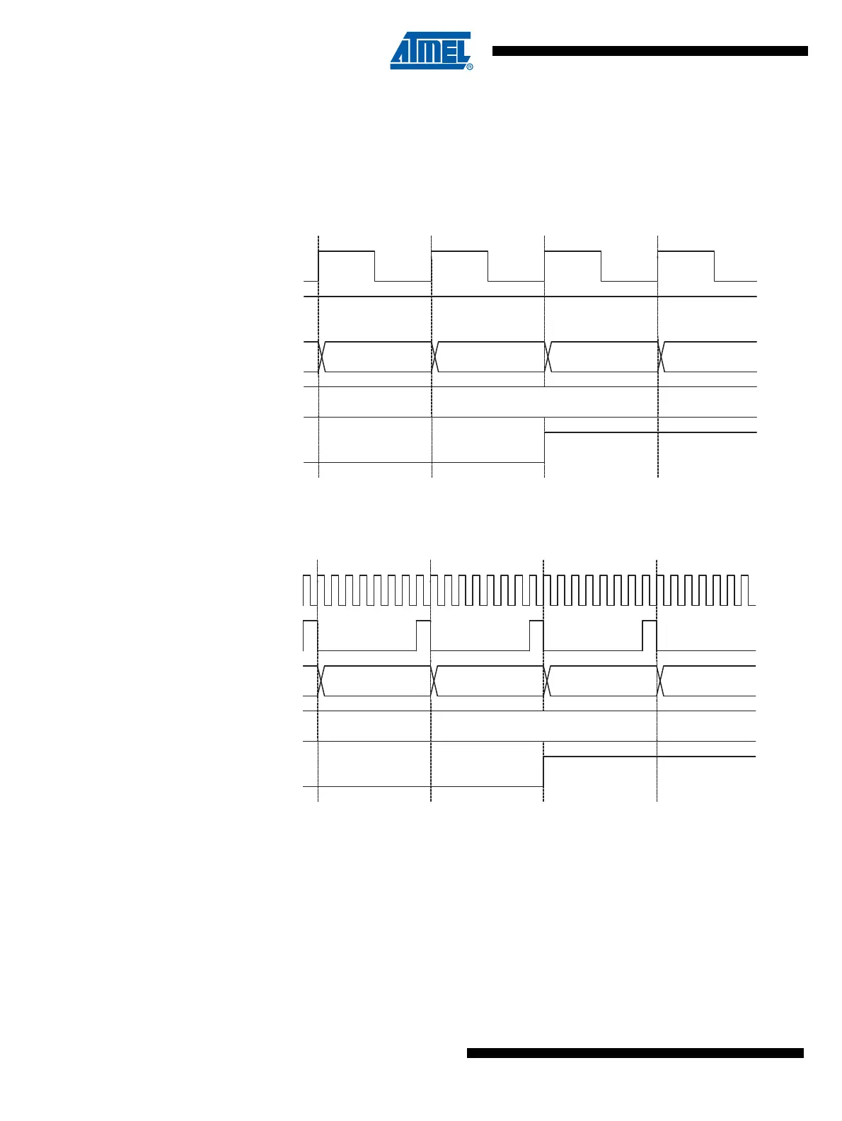
13.9 Timer/Counter Timing Diagrams
The Timer/Counter is a synchronous design and the timer clock (clk
Tn
) is therefore shown as a
clock enable signal in the following figures. The figures include information on when Interrupt
Flags are set, and when the OCRnx Register is updated with the OCRnx buffer value (only for
modes utilizing double buffering). Figure 13-10 shows a timing diagram for the setting of OCFnx.
Figure 13-10. Timer/Counter Timing Diagram, Setting of OCFnx, no Prescaling
Figure 13-11 shows the same timing data, but with the prescaler enabled.
Figure 13-11. Timer/Counter Timing Diagram, Setting of OCFnx, with Prescaler (f
clk_I/O
/8)
clk
Tn
(clk
I/O
/1)
OCFnx
clk
I/O
OCRnx
TCNTn
OCRnx Value
OCRnx - 1 OCRnx OCRnx + 1 OCRnx + 2
OCFnx
OCRnx
TCNTn
OCRnx Value
OCRnx - 1 OCRnx OCRnx + 1 OCRnx + 2
clk
I/O
clk
Tn
(clk
I/O
/8)