241
7647H–AVR–03/12
Atmel ATmega16/32/64/M1/C1
18.7 ADC Conversion Result
After the conversion is complete (ADIF is high), the conversion result can be found in the ADC
Result Registers (ADCL, ADCH).
For single ended conversion, the result is:
where V
IN
is the voltage on the selected input pin and V
REF
the selected voltage reference (see
Table 18-4 on page 245 and Table 18-5 on page 246). 0x000 represents analog ground, and
0x3FF represents the selected reference voltage.
If differential channels are used, the result is:
where V
POS
is the voltage on the positive input pin, V
NEG
the voltage on the negative input pin,
GAIN the selected gain factor and V
REF
the selected voltage reference. The result is presented
in two’s complement form, from 0x200 (-512d) through 0x1FF (+511d). Note that if the user
wants to perform a quick polarity check of the result, it is sufficient to read the MSB of the result
(ADC9 in ADCH). If the bit is one, the result is negative, and if this bit is zero, the result is posi-
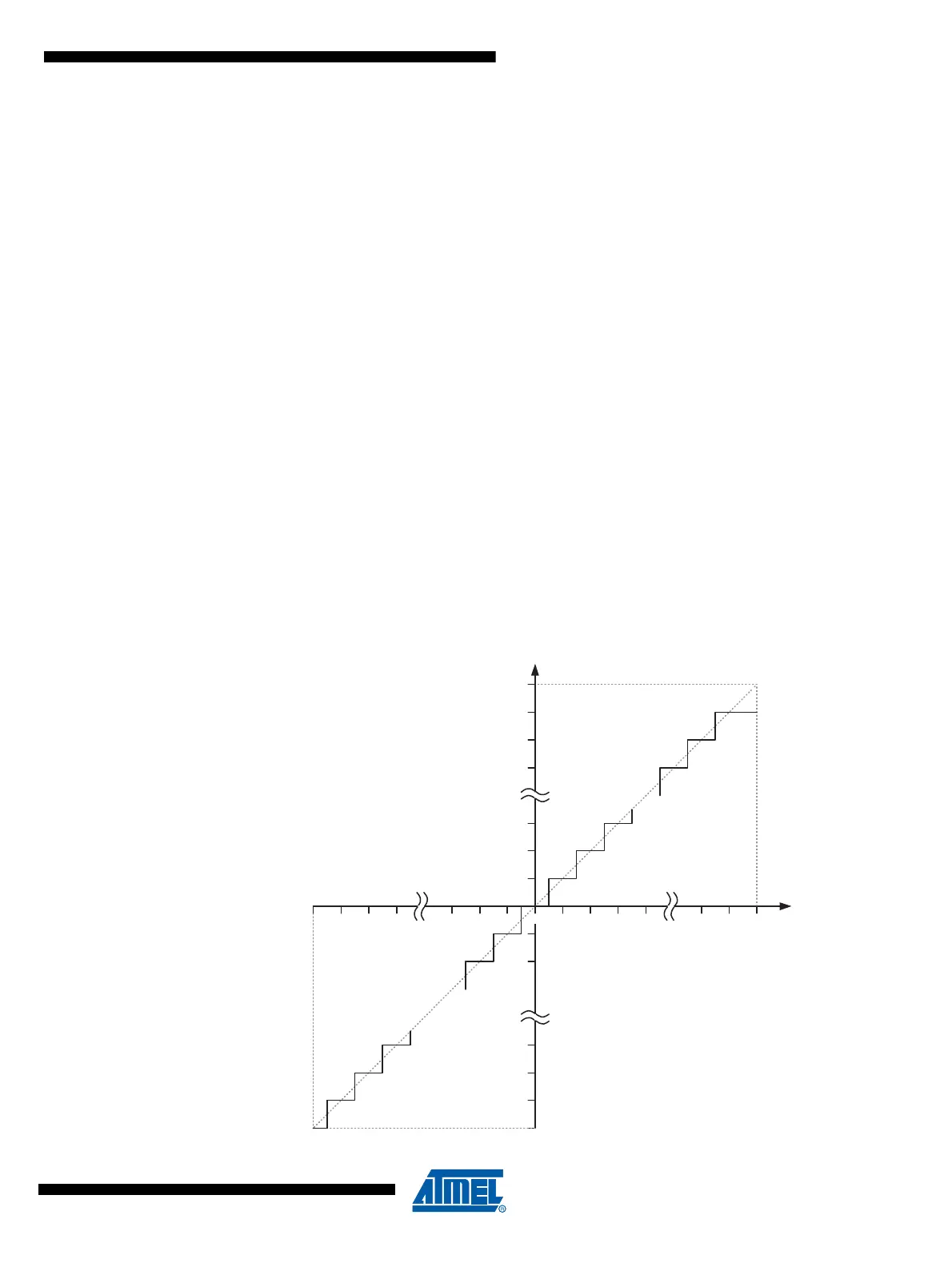
tive. Figure 18-13 shows the decoding of the differential input range.
Table 82 shows the resulting output codes if the differential input channel pair (ADCn - ADCm) is
selected with a reference voltage of V
REF
.
Figure 18-13. Differential Measurement Range
ADC
V
IN
1023⋅
V
REF
-----------------------------=
ADC
V
POS
V
NEG
–()GAIN 512⋅⋅
V
REF
------------------------------------------------------------------------------=
0
Output Code
0x1FF
0x000
V
REF
Differential Input
Voltage (Volts)
0x3FF
0x200
- V
REF
/Gain
/Gain