245
7647H–AVR–03/12
Atmel ATmega16/32/64/M1/C1
18.9 ADC Register Description
The ADC of the ATmega16/32/64/M1/C1 is controlled through 3 different registers. The ADC-
SRA and The ADCSRB registers which are the ADC Control and Status registers, and the
ADMUX which allows to select the Vref source and the channel to be converted.
The conversion result is stored on ADCH and ADCL register which contain respectively the most
significant bits and the less significant bits.
18.9.1 ADC Multiplexer Register – ADMUX
• Bit 7, 6 – REFS1, 0: ADC Vref Selection Bits
These 2 bits determine the voltage reference for the ADC.
The different setting are shown in Table 18-4.
If bits REFS1 and REFS0 are changed during a conversion, the change will not take effect until
this conversion is complete (it means while the ADIF bit in ADCSRA register is set).
In case the internal Vref is selected, it is turned ON as soon as an analog feature needed it is
set.
• Bit 5 – ADLAR: ADC Left Adjust Result
Set this bit to left adjust the ADC result.
Clear it to right adjust the ADC result.
The ADLAR bit affects the configuration of the ADC result data registers. Changing this bit
affects the ADC data registers immediately regardless of any on going conversion. For a com-
plete description of this bit, see Section “ADC Result Data Registers – ADCH and ADCL”,
page 249.
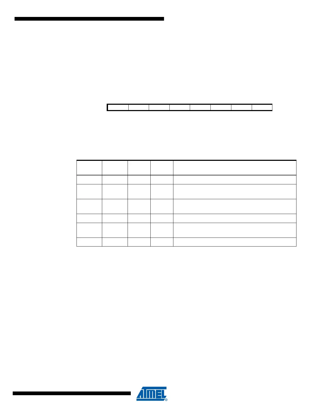
Bit 76543210
REFS1 REFS0 ADLAR MUX4 MUX3 MUX2 MUX1 MUX0 ADMUX
Read/Write R/W R/W R/W - R/W R/W R/W R/W
Initial Value 00000000
Table 18-4. ADC Voltage Reference Selection
AREFE
N ISRCEN REFS1 REFS0 Description
1 0 0 0 External Vref on AREF pin, Internal Vref is switched off
1001
AVcc with external capacitor connected on the AREF
pin
0001
AVcc (no external capacitor connected on the AREF
pin)
1 0 1 0 Reserved
1011
Internal 2.56V Reference voltage with external
capacitor connected on the AREF pin
0 x 1 1 Internal 2.56V Reference voltage