321
7647H–AVR–03/12
Atmel ATmega16/32/64/M1/C1
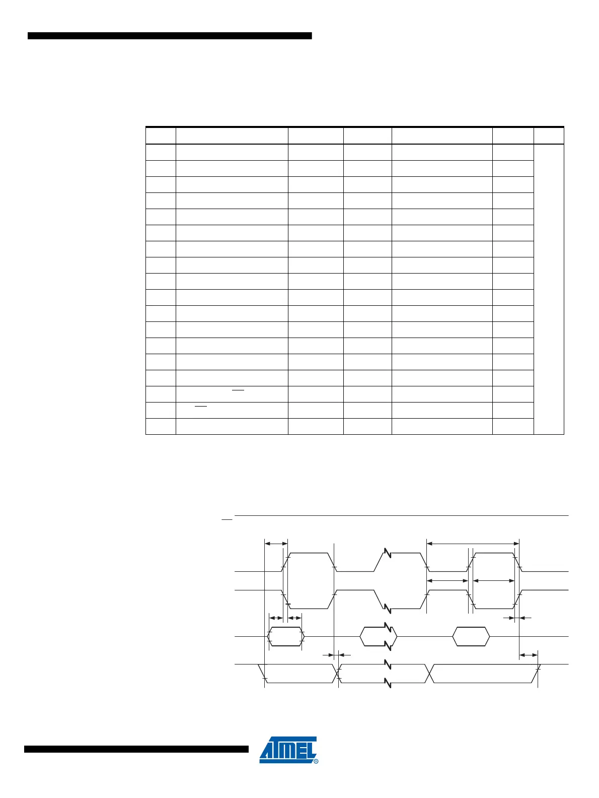
26.7 SPI Timing Characteristics
See Figure 26-3 and Figure 26-4 for details.
Note: In SPI Programming mode the minimum SCK high/low period is:
- 2 t
CLCL
for f
CK
< 12MHz
- 3 t
CLCL
for f
CK
>12MHz
Figure 26-3. SPI Interface Timing Requirements (Master Mode)
Table 26-4. SPI Timing Parameters
Description Mode Min. Typ. Max.
1 SCK period Master See Table 15-4
ns
2 SCK high/low Master 50% duty cycle
3 Rise/Fall time Master 3.6
4 Setup Master 10
5 Hold Master 10
6 Out to SCK Master 0.5 • t
sck
7 SCK to out Master 10
8 SCK to out high Master 10
9 SS low to out Slave 15
10 SCK period Slave 4 • t
ck
11 SCK high/low
(1)
Slave 2 • t
ck
12 Rise/Fall time Slave 1600
13 Setup Slave 10
14 Hold Slave t
ck
15 SCK to out Slave 15
16 SCK to SS high Slave 20
17 SS
high to tri-state Slave 10
18 SS low to SCK Slave 20
MOSI
(Data Output)
SCK
(CPOL = 1)
MISO
(Data Input)
SCK
(CPOL = 0)
SS
MSB LSB
LSBMSB
...
...
61
22
345
8
7