319
7647H–AVR–03/12
Atmel ATmega16/32/64/M1/C1
4. Although each I/O port can source more than the test conditions (10mA at V
CC
= 5V, 8mA at V
CC
= 3V) under steady state
conditions (non-transient), the following must be observed:
1] The sum of all IOH, for ports B0 - B1, C2 - C3, D4, E1 - E2 should not exceed 100mA.
2] The sum of all IOH, for ports B6 - B7, C0 - C1, D0 -D3, E0 should not exceed 100mA.
3] The sum of all IOH, for ports B2 - B5, C4 - C7, D5 - D7 should not exceed 100mA.
If IOH exceeds the test condition, VOH may exceed the related specification. Pins are not guaranteed to source current
greater than the listed test condition.
5. Minimum V
CC
for Power-down is 2.5V.
6. The Analog Comparator Propogation Delay equals 1 comparator clock plus 30nS. See “Analog Comparator” on page 262.
for comparator clock definition.
26.3 Clock Characteristics
26.3.1 Calibrated Internal RC Oscillator Accuracy
26.4 External Clock Drive Characteristics
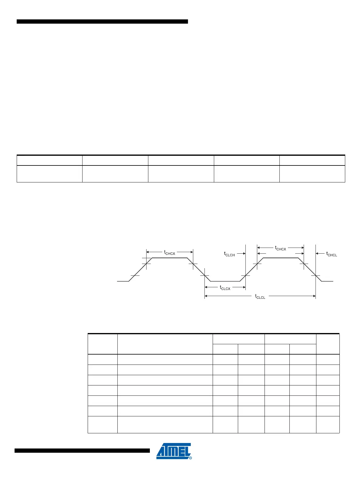
Figure 26-1. External Clock Drive Waveforms
Table 26-1. Calibration Accuracy of Internal RC Oscillator
Frequency V
CC
Temperature Calibration Accuracy
Factory
Calibration
8.0MHz 3V 25°C ±2%
Table 26-2. External Clock Drive
Symbol Parameter
V
CC
= 2.7 - 5.5V V
CC
= 4.5 - 5.5V
UnitsMin. Max. Min. Max.
1/t
CLCL
Oscillator Frequency 0 8 0 16 MHz
t
CLCL
Clock Period 125 62.5 ns
t
CHCX
High Time 50 25 ns
t
CLCX
Low Time 50 25 ns
t
CLCH
Rise Time 1.6 0.5 µs
t
CHCL
Fall Time 1.6 0.5 µs
Δt
CLCL
Change in period from one clock
cycle to the next
22%

 Loading...


