28
7647H–AVR–03/12
Atmel ATmega16/32/64/M1/C1
4.4 I/O Memory
The I/O space definition of the ATmega16/32/64/M1/C1 is shown in “Register Summary” on
page 347.
All ATmega16/32/64/M1/C1 I/Os and peripherals are placed in the I/O space. All I/O locations
may be accessed by the LD/LDS/LDD and ST/STS/STD instructions, transferring data between
the 32 general purpose working registers and the I/O space. I/O registers within the address
range 0x00 - 0x1F are directly bit-accessible using the SBI and CBI instructions. In these regis-
ters, the value of single bits can be checked by using the SBIS and SBIC instructions. Refer to
the instruction set section for more details. When using the I/O specific commands IN and OUT,
the I/O addresses 0x00 - 0x3F must be used. When addressing I/O registers as data space
using LD and ST instructions, 0x20 must be added to these addresses. The
ATmega16/32/64/M1/C1 is a complex microcontroller with more peripheral units than can be
supported within the 64 location reserved in Opcode for the IN and OUT instructions. For the
Extended I/O space from 0x60 - 0xFF in SRAM, only the ST/STS/STD and LD/LDS/LDD instruc-
tions can be used.
For compatibility with future devices, reserved bits should be written to zero if accessed.
Reserved I/O memory addresses should never be written.
Some of the status flags are cleared by writing a logical one to them. Note that, unlike most other
AVR’s, the CBI and SBI instructions will only operate on the specified bit, and can therefore be
used on registers containing such status flags. The CBI and SBI instructions work with registers
0x00 to 0x1F only.
The I/O and peripherals control registers are explained in later sections.
4.5 General Purpose I/O Registers
The ATmega16/32/64/M1/C1 contains four General Purpose I/O Registers. These registers can
be used for storing any information, and they are particularly useful for storing global variables
and status flags.
The General Purpose I/O Registers, within the address range 0x00 - 0x1F, are directly
bit-accessible using the SBI, CBI, SBIS, and SBIC instructions.
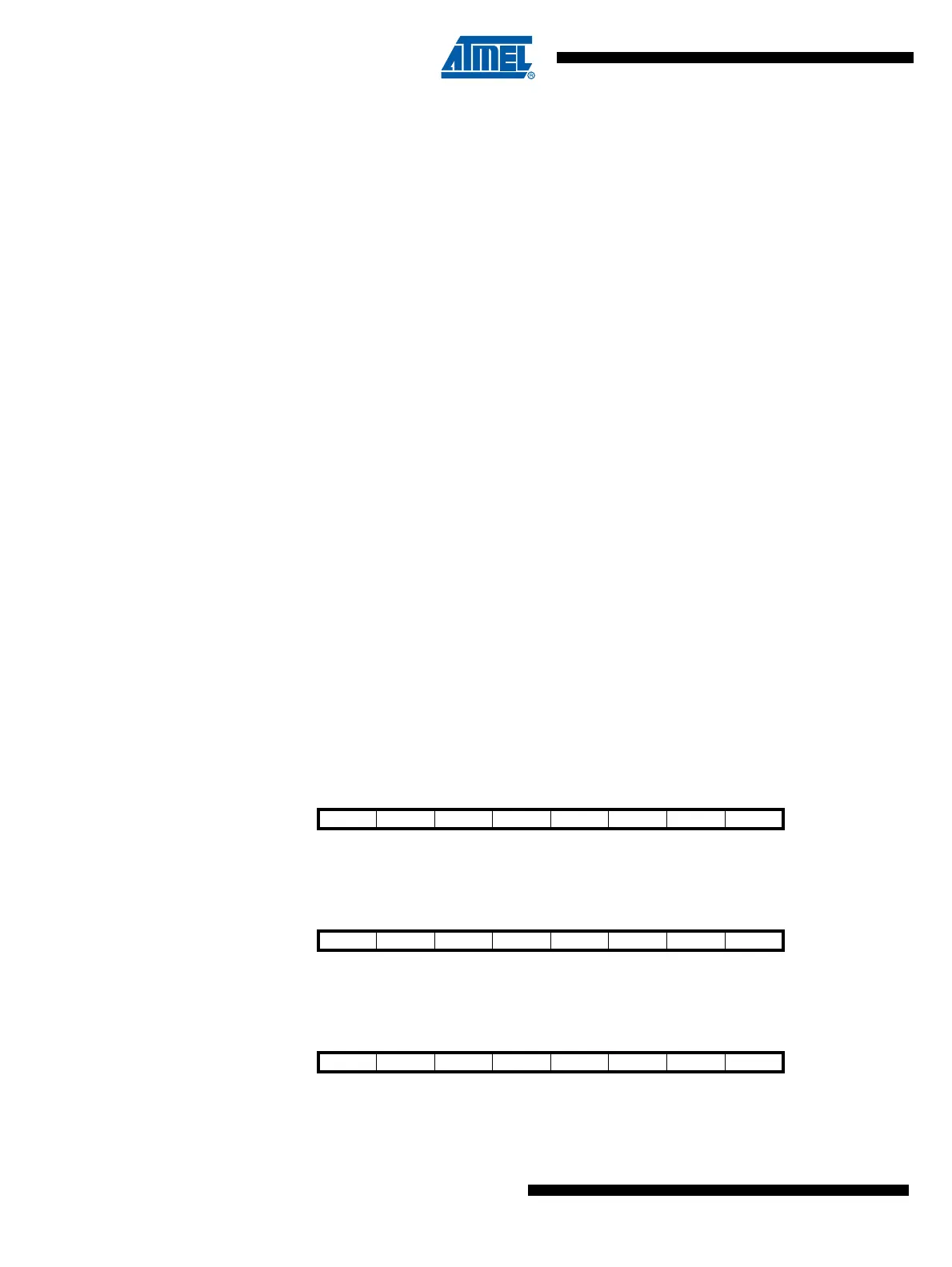
4.5.1 General Purpose I/O Register 0 – GPIOR0
4.5.2 General Purpose I/O Register 1 – GPIOR1
4.5.3 General Purpose I/O Register 2 – GPIOR2
Bit 76543210
GPIOR07 GPIOR06 GPIOR05 GPIOR04 GPIOR03 GPIOR02 GPIOR01 GPIOR00 GPIOR0
Read/Write R/W R/W R/W R/W R/W R/W R/W R/W
Initial Value00000000
Bit 76543210
GPIOR17 GPIOR16 GPIOR15 GPIOR14 GPIOR13 GPIOR12 GPIOR11 GPIOR10 GPIOR1
Read/Write R/W R/W R/W R/W R/W R/W R/W R/W
Initial Value00000000
Bit 76543210
GPIOR27 GPIOR26 GPIOR25 GPIOR24 GPIOR23 GPIOR22 GPIOR21 GPIOR20 GPIOR2
Read/Write R/W R/W R/W R/W R/W R/W R/W R/W
Initial Value00000000