EasyManua.ls Logo

Atmel ATmega32M1 User Manual

Atmel ATmega32M1
367 pages
To Next Page IconTo Next Page
To Previous Page IconTo Previous Page
Page #20 background imageLoading...
Page #20 background image
20
7647H–AVR–03/12
Atmel ATmega16/32/64/M1/C1
4. Memories
This section describes the different memories in the ATmega16/32/64/M1/C1. The AVR archi-
tecture has two main memory spaces, the Data Memory and the Program Memory space. In
addition, the ATmega16/32/64/M1/C1 features an EEPROM Memory for data storage. All three
memory spaces are linear and regular.
4.1 In-System Reprogrammable Flash Program Memory
The ATmega16/32/64/M1/C1 contains 16K/32K/64K bytes On-chip In-System Reprogrammable
Flash memory for program storage. Since all AVR instructions are 16 or 32 bits wide, the Flash
is organized as 8K x 16, 16K x 16 , 32K x 16. For software security, the Flash Program memory
space is divided into two sections, Boot Program section and Application Program section.
The Flash memory has an endurance of at least 10,000 write/erase cycles. The
ATmega16/32/64/M1/C1 Program Counter (PC) is 14/15 bits wide, thus addressing the
8K/16K/32K program memory locations. The operation of Boot Program section and associated
Boot Lock bits for software protection are described in detail in Boot Loader Support –
Read-While-Write Self-Programming ATmega16/32/64/M1/C1” on page 279. “Memory Program-
ming” on page 296 contains a detailed description on Flash programming in SPI or Parallel
programming mode.
Constant tables can be allocated within the entire program memory address space (see the LPM
– Load Program Memory.
Timing diagrams for instruction fetch and execution are presented in Instruction Execution Tim-
ing” on page 17.
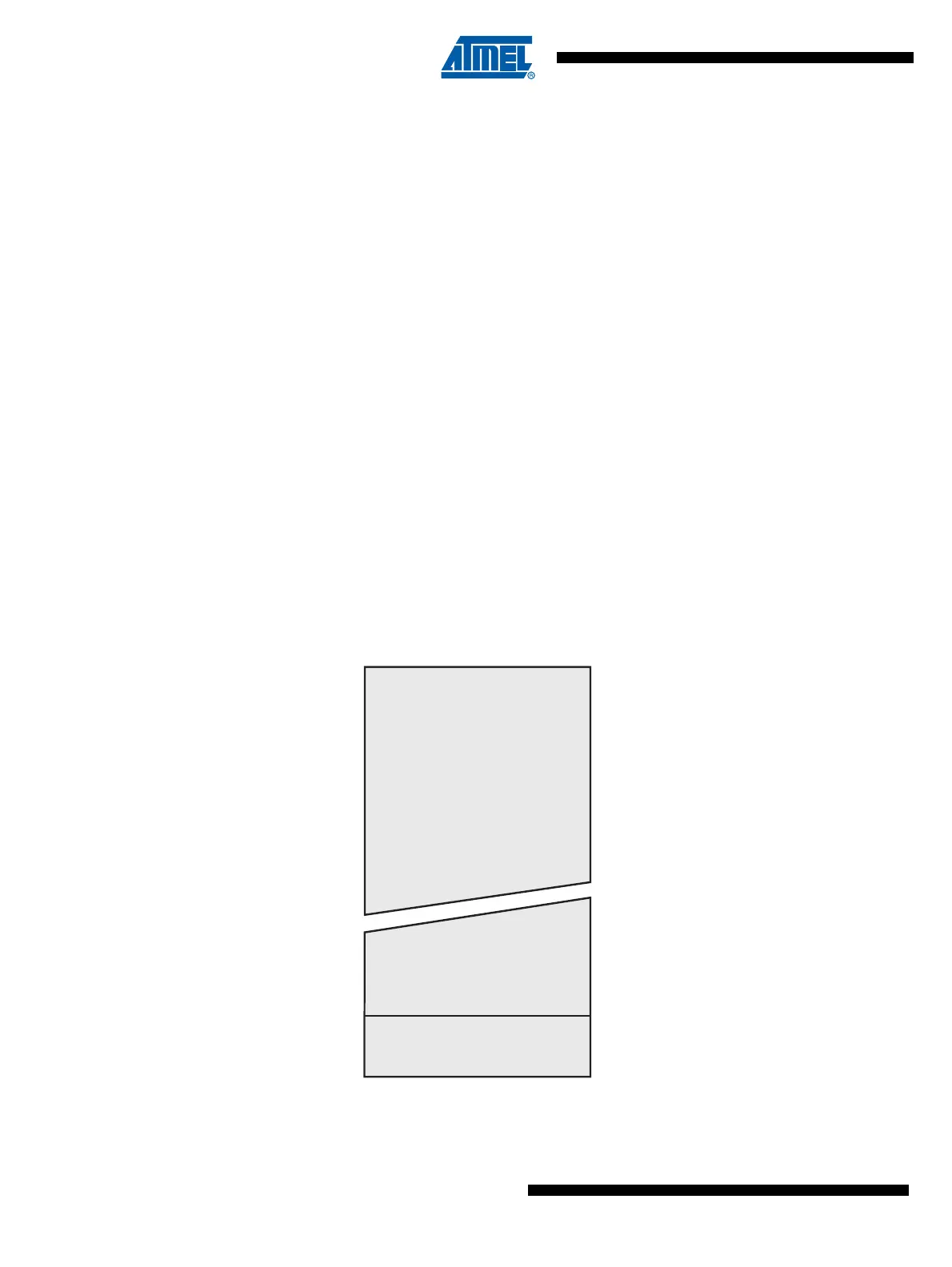
Figure 4-1. Program Memory Map
0x0000
0x1FFF/0x3FFF/0x7
F
Program Memory
Application Flash Section
Boot Flash Section

Table of Contents

Question and Answer IconNeed help?

Do you have a question about the Atmel ATmega32M1 and is the answer not in the manual?

Atmel ATmega32M1 Specifications

General IconGeneral
Architecture8-bit AVR
Flash Memory32 KB
SRAM2 KB
EEPROM1 KB
Clock Speed16 MHz
GPIO Pins32
I/O Pins32
ADC Channels8
ADC Resolution10-bit
UART1
USART1
SPI1
I2C1
PWM Channels6
CAN1
Operating Voltage2.7V - 5.5V
Operating Temperature-40°C to +85°C
Temperature Range-40°C to +85°C
Package44-TQFP, 44-QFN

Summary

Features

AVR CPU Core

Reset and Interrupt Handling

Explanation of interrupt sources, vectors, priority levels, and behavior during interrupt execution.

System Clock

System Clock Prescaler

Details on the CLKPR register for dividing the system clock to reduce power consumption and affect peripheral frequencies.

Power Management and Sleep Modes

8-bit Timer/Counter0 with PWM

Modes of Operation

Detailed explanation of Normal, CTC, and various PWM modes for Timer/Counter0 operation.

Controller Area Network - CAN

CAN Protocol

Explanation of the CAN protocol principles, standards, and message transmission priorities.

Error Management

Description of error detection mechanisms (message and bit level) and fault confinement states.

Analog to Digital Converter - ADC

Features

List of ADC capabilities including resolution, accuracy, conversion time, input channels, and reference voltages.

Starting a Conversion

Procedures for initiating ADC conversions, including single conversion and auto-triggering modes.

debugWIRE On-chip Debug System

Features

Overview of debugWIRE capabilities including program flow control, real-time operation, and symbolic debugging.

Boot Loader Support – Read-While-Write Self-Programming ATmega16/32/64/M1/C1

Self-Programming the Flash

Procedures and considerations for programming the Flash memory using the SPM instruction.

Memory Programming

Electrical Characteristics

Absolute Maximum Ratings*

Critical voltage, current, and temperature limits that must not be exceeded for device reliability.

Instruction Set Summary

Register Summary

Related product manuals