67
7647H–AVR–03/12
Atmel ATmega16/32/64/M1/C1
9.3 Alternate Port Functions
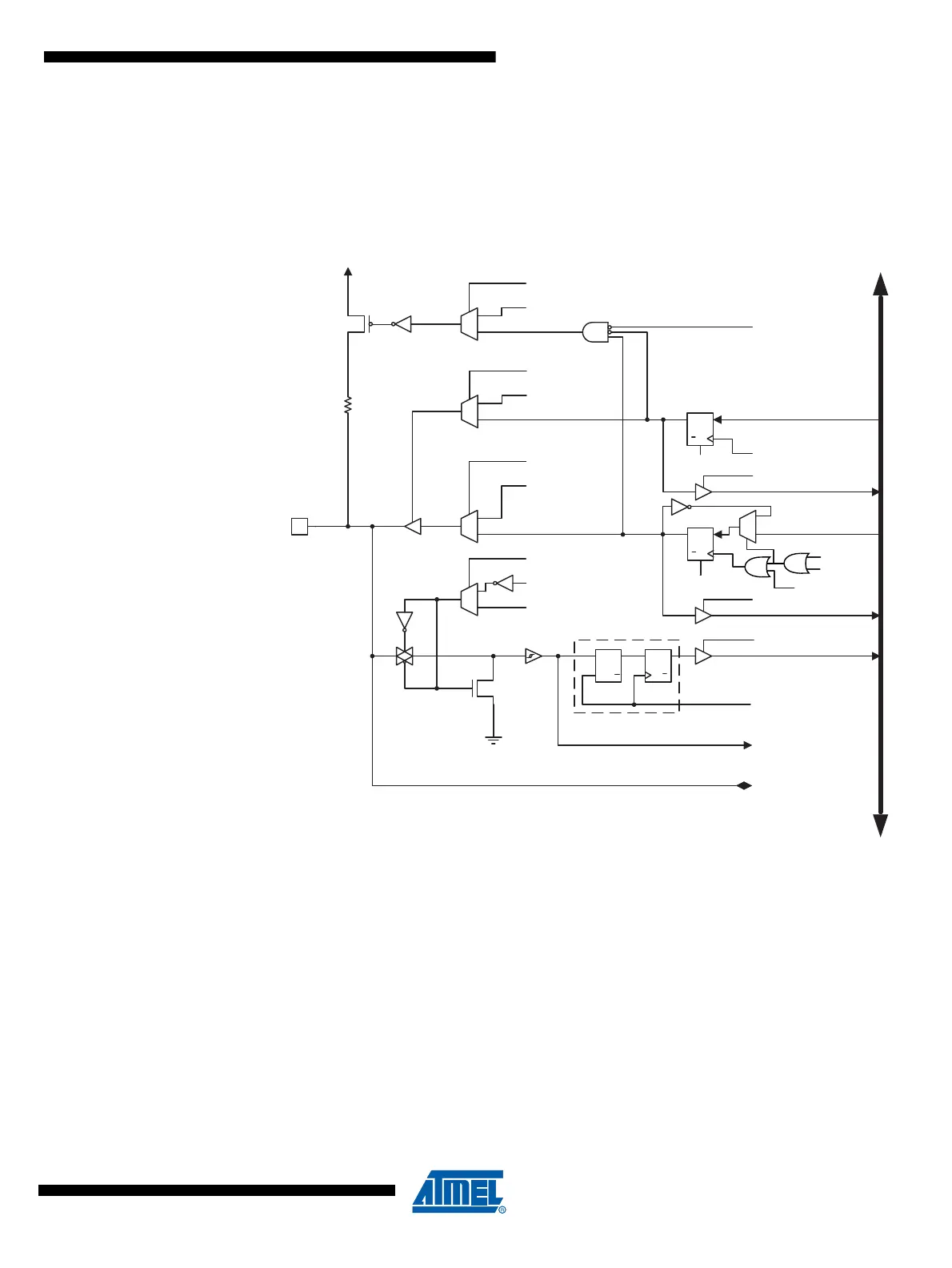
Most port pins have alternate functions in addition to being general digital I/Os. Figure 9-5 shows
how the port pin control signals from the simplified Figure 9-2 can be overridden by alternate
functions. The overriding signals may not be present in all port pins, but the figure serves as a
generic description applicable to all port pins in the AVR microcontroller family.
Figure 9-5. Alternate Port Functions
(1)
Note: 1. WRx, WPx, WDx, RRx, RPx, and RDx are common to all pins within the same port. clk
I/O
,
SLEEP, and PUD are common to all ports. All other signals are unique for each pin.
Table 9-2 summarizes the function of the overriding signals. The pin and port indexes from Fig-
ure 9-5 are not shown in the succeeding tables. The overriding signals are generated internally
in the modules having the alternate function.
clk
RPx
RRx
WRx
RDx
WDx
PUD
SYNCHRONIZER
WDx: WRITE DDRx
WRx: WRITE PORTx
RRx: READ PORTx REGISTER
RPx: READ PORTx PIN
PUD: PULLUP DISABLE
clk
I/O
: I/O CLOCK
RDx: READ DDRx
D
L
Q
Q
SET
CLR
0
1
0
1
0
1
DIxn
AIOxn
DIEOExn
PVOVxn
PVOExn
DDOVxn
DDOExn
PUOExn
PUOVxn
PUOExn: Pxn PULL-UP OVERRIDE ENABLE
PUOVxn: Pxn PULL-UP OVERRIDE VALUE
DDOExn: Pxn DATA DIRECTION OVERRIDE ENABLE
DDOVxn: Pxn DATA DIRECTION OVERRIDE VALUE
PVOExn: Pxn PORT VALUE OVERRIDE ENABLE
PVOVxn: Pxn PORT VALUE OVERRIDE VALUE
DIxn: DIGITAL INPUT PIN n ON PORTx
AIOxn: ANALOG INPUT/OUTPUT PIN n ON PORTx
RESET
RESET
Q
Q
D
CLR
Q
Q
D
CLR
Q
Q
D
CLR
PINxn
PORTxn
DDxn
DATA BUS
0
1
DIEOVxn
SLEEP
DIEOExn: Pxn DIGITAL INPUT-ENABLE OVERRIDE ENABLE
DIEOVxn: Pxn DIGITAL INPUT-ENABLE OVERRIDE VALUE
SLEEP: SLEEP CONTROL
Pxn
I/O
0
1
PTOExn
WPx
PTOExn: Pxn, PORT TOGGLE OVERRIDE ENABLE
WPx: WRITE PINx