5
7647H–AVR–03/12
Atmel ATmega16/32/64/M1/C1
1.1 Pin Descriptions
:
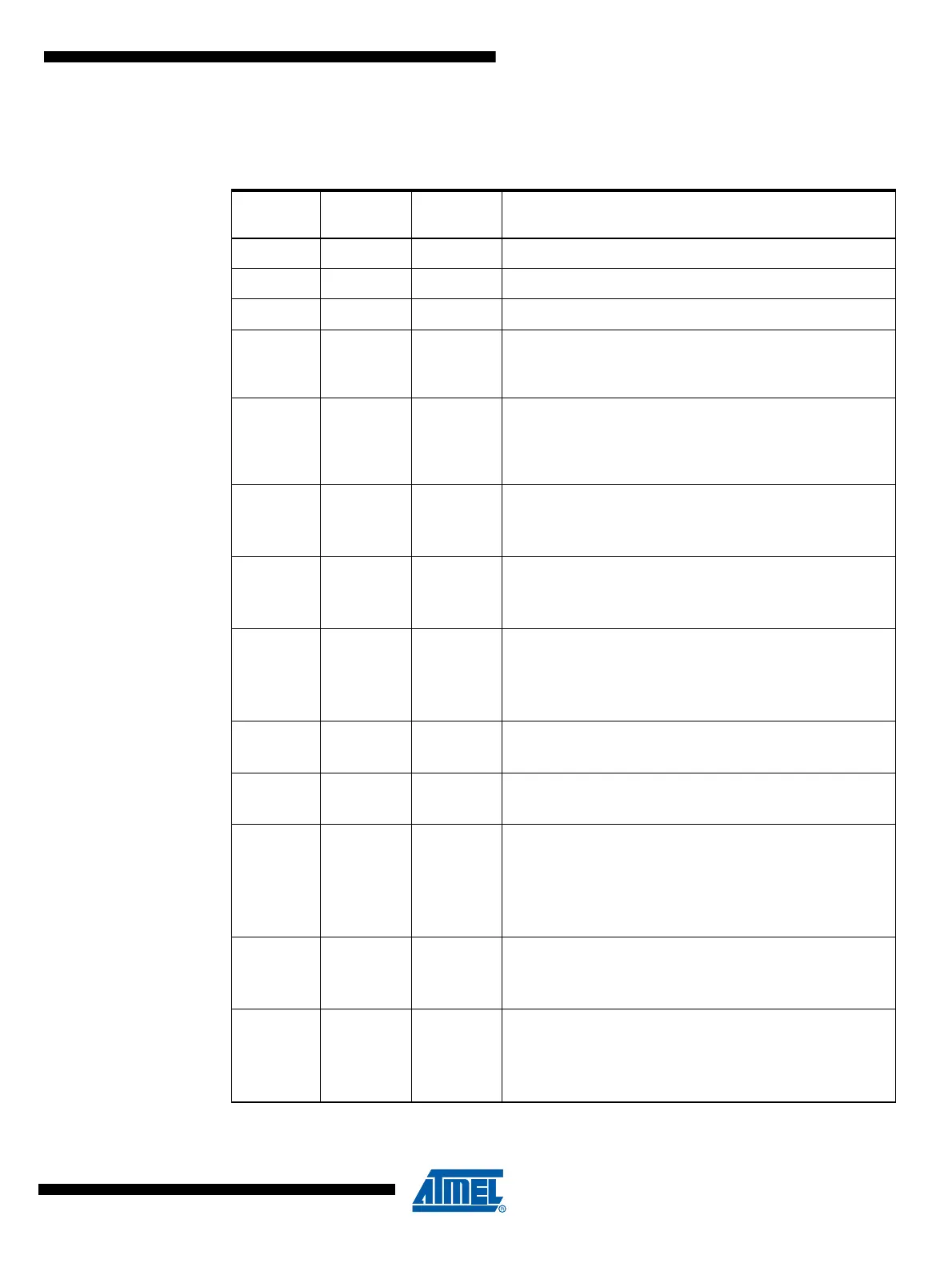
Table 1-1. Pin out description
QFN32 Pin
Number Mnemonic Type Name, Function and Alternate Function
5GNDPowerGround: 0V reference
20 AGND Power Analog Ground: 0V reference for analog part
4 VCC Power Power Supply
19 AVCC Power
Analog Power Supply: This is the power supply voltage for
analog part
For a normal use this pin must be connected.
21 AREF Power
Analog Reference : reference for analog converter . This is
the reference voltage of the A/D converter. As output, can be
used by external analog
ISRC (Current Source Output)
8 PB0 I/O
MISO (SPI Master In Slave Out)
PSCOUT2A (PSC Module 2 Output A)
PCINT0 (Pin Change Interrupt 0)
9 PB1 I/O
MOSI (SPI Master Out Slave In)
PSCOUT2B (PSC Module 2 Output B)
PCINT1 (Pin Change Interrupt 1)
16 PB2 I/O
ADC5 (Analog Input Channel 5 )
INT1 (External Interrupt 1 Input)
ACMPN0 (Analog Comparator 0 Negative Input)
PCINT2 (Pin Change Interrupt 2)
23 PB3 I/O
AMP0- (Analog Differential Amplifier 0 Negative Input)
PCINT3 (Pin Change Interrupt 3)
24 PB4 I/O
AMP0+ (Analog Differential Amplifier 0 Positive Input)
PCINT4 (Pin Change Interrupt 4)
26 PB5 I/O
ADC6 (Analog Input Channel 6)
INT2 (External Interrupt 2 Input)
ACMPN1 (Analog Comparator 1 Negative Input)
AMP2- (Analog Differential Amplifier 2 Negative Input)
PCINT5 (Pin Change Interrupt 5)
27 PB6 I/O
ADC7 (Analog Input Channel 7)
PSCOUT1B (PSC Module 1 Output A)
PCINT6 (Pin Change Interrupt 6)
28 PB7 I/O
ADC4 (Analog Input Channel 4)
PSCOUT0B (PSC Module 0 Output B)
SCK (SPI Clock)
PCINT7 (Pin Change Interrupt 7)
Note: 1. On the first engineering samples (Parts marked AT90PWM324), the ACMPN3 alternate
function is not located on PC4. It is located on PE2.