223
7647H–AVR–03/12
Atmel ATmega16/32/64/M1/C1
17.6 LIN / UART Register Description
17.6.1 LIN Control Register - LINCR
• Bit 7 - LSWRES: Software Reset
– 0 = No action,
– 1 = Software reset (this bit is self-reset at the end of the reset procedure).
• Bit 6 - LIN13: LIN 1.3 mode
– 0 = LIN 2.1 (default),
– 1 = LIN 1.3.
• Bit 5:4 - LCONF[1:0]: Configuration
a. LIN mode (default = 00):
– 00 = LIN Standard configuration (listen mode “off”, CRC “on” & Frame_Time_Out
“on”,
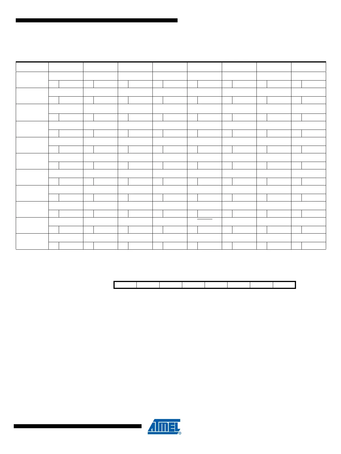
Table 17-5. LIN/UART Register Bits Summary
Name Bit 7 Bit 6 Bit 5 Bit 4 Bit 3 Bit 2 Bit 1 Bit 0
LINCR
LSWRES LIN13 LCONF1 LCONF0 LENA LCMD2 LCMD1 LCMD0
0R/W0R/W0R/W0R/W0R/W0R/W0R/W0R/W
LINSIR
LIDST2 LIDST1 LIDST0 LBUSY LERR LIDOK LTXOK LRXOK
0R0R0R0R0R/W
one
0R/W
one
0R/W
one
0R/W
one
LINENIR
— — — — LENERR LENIDOK LENTXOK LENRXOK
0 R 0 R 0 R 0 R 0R/W0R/W0R/W0R/W
LINERR
LABORT LTOERR LOVERR LFERR LSERR LPERR LCERR LBERR
0R0R0R0R0R0R0R0R
LINBTR
LDISR LBT5 LBT4 LBT3 LBT2 LBT1 LBT0
0 R/W 0 R 1 R/(W) 0 R/(W) 0 R/(W) 0 R/(W) 0 R/(W) 0 R/(W)
LINBRRL
LDIV7 LDIV6 LDIV5 LDIV4 LDIV3 LDIV2 LDIV1 LDIV0
0R/W0R/W0R/W0R/W0R/W0R/W0R/W0R/W
LINBRRH
— — — — LDIV11 LDIV10 LDIV9 LDIV8
0 R 0 R 0 R 0 R 0R/W0R/W0R/W0R/W
LINDLR
LTXDL3 LTXDL2 LTXDL1 LTXDL0 LRXDL3 LRXDL2 LRXDL1 LRXDL0
0R/W0R/W0R/W0R/W0R/W0R/W0R/W0R/W
LINIDR
LP1 LP0 LID5/LDL1 LID4/LDL0 LID3 LID2 LID1 LID0
1 R 0 R 0R/W0R/W0R/W0R/W0R/W0R/W
LINSEL
————LAINC
LINDX2 LINDX1 LINDX0
0 R 0 R 0 R 0 R 0R/W0R/W0R/W0R/W
LINDAT
LDATA7 LDATA6 LDATA5 LDATA4 LDATA3 LDATA2 LDATA1 LDATA0
0R/W0R/W0R/W0R/W0R/W0R/W0R/W0R/W
Bit 76543210
LSWRES LIN13 LCONF1 LCONF0 LENA LCMD2 LCMD1 LCMD0
LINCR
Read/Write R/W R/W R/W R/W R/W R/W R/W R/W
Initial Value00000000