EasyManua.ls Logo

Atmel ATmega32M1 User Manual

Atmel ATmega32M1
367 pages
To Next Page IconTo Next Page
To Previous Page IconTo Previous Page
Page #286 background imageLoading...
Page #286 background image
286
7647H–AVR–03/12
Atmel ATmega16/32/64/M1/C1
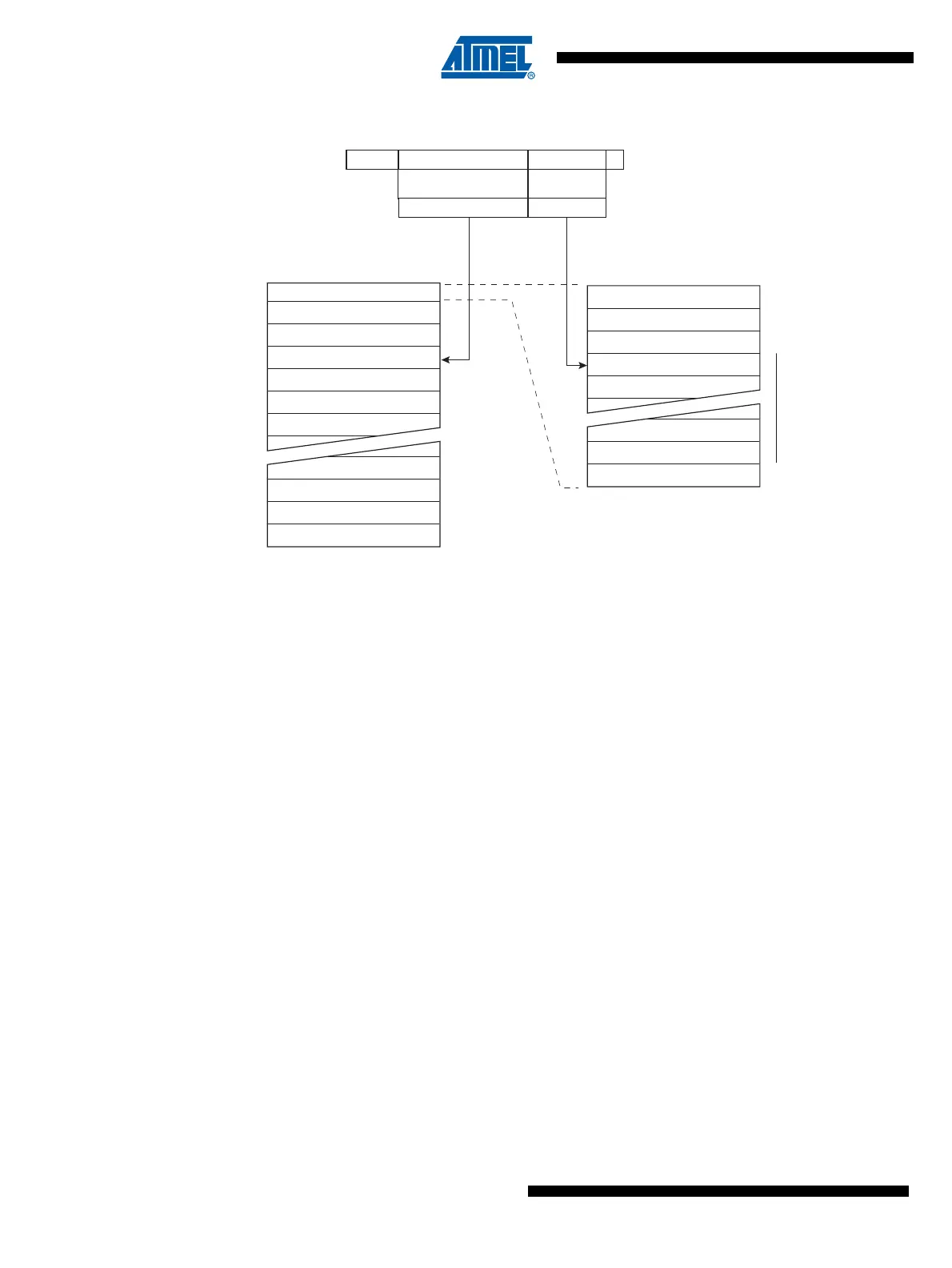
Figure 24-3. Addressing the Flash During SPM
(1)
Note: 1. The different variables used in Figure 24-3 are listed in Table 24-9 on page 293.
24.7 Self-Programming the Flash
The program memory is updated in a page by page fashion. Before programming a page with
the data stored in the temporary page buffer, the page must be erased. The temporary page buf-
fer is filled one word at a time using SPM and the buffer can be filled either before the Page
Erase command or between a Page Erase and a Page Write operation:
Alternative 1, fill the buffer before a Page Erase
Fill temporary page buffer
Perform a Page Erase
Perform a Page Write
Alternative 2, fill the buffer after Page Erase
Perform a Page Erase
Fill temporary page buffer
Perform a Page Write
If only a part of the page needs to be changed, the rest of the page must be stored (for example
in the temporary page buffer) before the erase, and then be rewritten. When using alternative 1,
the Boot Loader provides an effective Read-Modify-Write feature which allows the user software
to first read the page, do the necessary changes, and then write back the modified data. If alter-
native 2 is used, it is not possible to read the old data while loading since the page is already
erased. The temporary page buffer can be accessed in a random sequence. It is essential that
the page address used in both the Page Erase and Page Write operation is addressing the same
page. See “Simple Assembly Code Example for a Boot Loader” on page 290 for an assembly
code example.
PROGRAM MEMORY
0115
Z - REGISTER
BIT
0
ZPAGEMSB
WORD ADDRESS
WITHIN A PAGE
PAGE ADDRESS
WITHIN THE FLASH
ZPCMSB
INSTRUCTION WORD
PAGE
PCWORD[PAGEMSB:0]:
00
01
02
PAGEEND
PAGE
PCWORDPCPAGE
PCMSB
PAGEMSB
PROGRAM
COUNTER

Table of Contents

Question and Answer IconNeed help?

Do you have a question about the Atmel ATmega32M1 and is the answer not in the manual?

Atmel ATmega32M1 Specifications

General IconGeneral
Architecture8-bit AVR
Flash Memory32 KB
SRAM2 KB
EEPROM1 KB
Clock Speed16 MHz
GPIO Pins32
I/O Pins32
ADC Channels8
ADC Resolution10-bit
UART1
USART1
SPI1
I2C1
PWM Channels6
CAN1
Operating Voltage2.7V - 5.5V
Operating Temperature-40°C to +85°C
Temperature Range-40°C to +85°C
Package44-TQFP, 44-QFN

Summary

Features

AVR CPU Core

Reset and Interrupt Handling

Explanation of interrupt sources, vectors, priority levels, and behavior during interrupt execution.

System Clock

System Clock Prescaler

Details on the CLKPR register for dividing the system clock to reduce power consumption and affect peripheral frequencies.

Power Management and Sleep Modes

8-bit Timer/Counter0 with PWM

Modes of Operation

Detailed explanation of Normal, CTC, and various PWM modes for Timer/Counter0 operation.

Controller Area Network - CAN

CAN Protocol

Explanation of the CAN protocol principles, standards, and message transmission priorities.

Error Management

Description of error detection mechanisms (message and bit level) and fault confinement states.

Analog to Digital Converter - ADC

Features

List of ADC capabilities including resolution, accuracy, conversion time, input channels, and reference voltages.

Starting a Conversion

Procedures for initiating ADC conversions, including single conversion and auto-triggering modes.

debugWIRE On-chip Debug System

Features

Overview of debugWIRE capabilities including program flow control, real-time operation, and symbolic debugging.

Boot Loader Support – Read-While-Write Self-Programming ATmega16/32/64/M1/C1

Self-Programming the Flash

Procedures and considerations for programming the Flash memory using the SPM instruction.

Memory Programming

Electrical Characteristics

Absolute Maximum Ratings*

Critical voltage, current, and temperature limits that must not be exceeded for device reliability.

Instruction Set Summary

Register Summary

Related product manuals