317
7647H–AVR–03/12
Atmel ATmega16/32/64/M1/C1
26. Electrical Characteristics
All DC/AC characteristics contained in this datasheet are based on simulations and character-
ization of similar devices in the same process and design methods. These values are
preliminary representing design targets, and will be updated after characterization of actual
automotive silicon data.
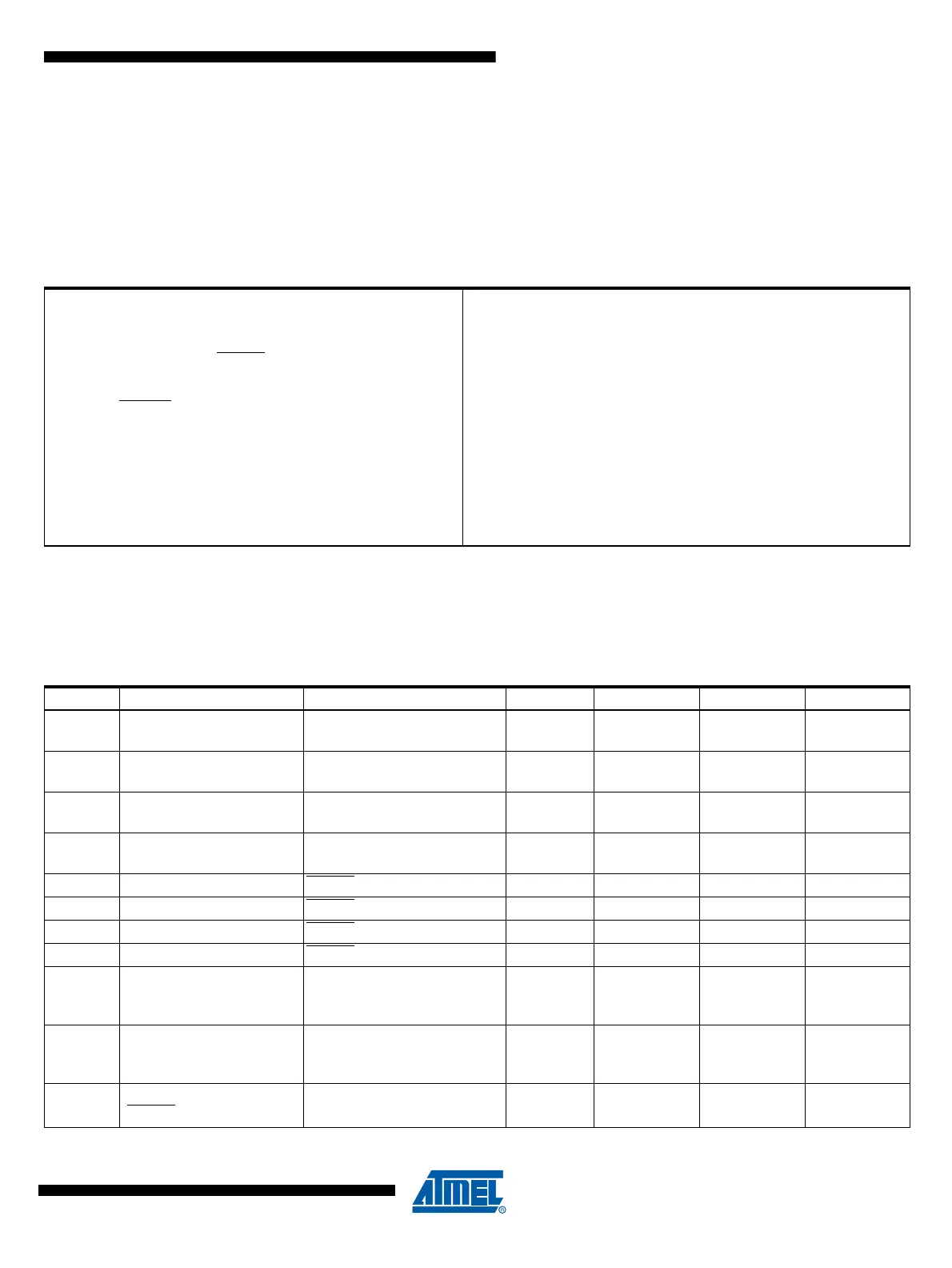
26.1 Absolute Maximum Ratings*
26.2 DC Characteristics
Operating Temperature ................................. –40°C to +125°C
*NOTICE: Stresses beyond those listed under “Absolute Max-
imum Ratings” may cause permanent damage to
the device. This is a stress rating only and func-
tional operation of the device at these or other con-
ditions beyond those indicated in the operational
sections of this specification is not implied. Expo-
sure to absolute maximum rating conditions for
extended periods may affect device reliability.
Storage Temperature..................................... –65°C to +150°C
Voltage on any Pin except RESET
with respect to Ground............................... –0.5V to V
CC
+0.5V
Voltage on RESET
with respect to Ground .... –0.5V to +13.0V
Maximum Operating Voltage .............................................6.0V
DC Current per I/O Pin.................................................40.0mA
DC Current
V
CC
and GND Pins .................................200.0mA
Injection Current at V
CC
= 0V to 5V...........................±5.0mA
(1)
Note: 1. Maximum current per port = ±30mA
T
A
= -40°C to +125°C, V
CC
= 2.7V to 5.5V (unless otherwise noted)
Symbol Parameter Condition Min. Typ. Max. Units
V
IL
Input Low Voltage
Port B, C & D and XTAL1,
XTAL2 pins as I/O
–0.5 0.2V
CC
(1)
V
V
IH
Input High Voltage
Port B, C & D and XTAL1,
XTAL2 pins as I/O
0.6V
CC
(2)
V
CC
+0.5 V
V
IL1
Input Low Voltage
XTAL1 pin , External Clock
Selected
–0.5 0.1V
CC
(1)
V
V
IH1
Input High Voltage
XTAL1 pin , External Clock
Selected
0.8V
CC
(2)
V
CC
+0.5 V
V
IL2
Input Low Voltage RESET pin –0.5 0.2V
CC
(1)
V
V
IH2
Input High Voltage RESET pin 0.9V
CC
(2)
V
CC
+0.5 V
V
IL3
Input Low Voltage RESET pin as I/O –0.5 0.2V
CC
(1)
V
V
IH3
Input High Voltage RESET pin as I/O 0.8V
CC
(2)
V
CC
+0.5 V
V
OL
Output Low Voltage
(3)
(Port B, C & D and XTAL1,
XTAL2 pins as I/O)
I
OL
= 10mA, V
CC
= 5V
I
OL
= 6mA, V
CC
= 3V
0.7
0.5
V
V
V
OH
Output High Voltage
(4)
(Port B, C & D and XTAL1,
XTAL2 pins as I/O)
I
OH
= –10mA, V
CC
= 5V
I
OH
= –8mA, V
CC
= 3V
4.2
2.2
V
V
V
OL3
Output Low Voltage
(3)
(RESET pin as I/O)
I
OL
= 2.1mA, V
CC
= 5V
I
OL
= 0.8mA, V
CC
= 3V
0.9
0.7
V
V