90
7647H–AVR–03/12
Atmel ATmega16/32/64/M1/C1
12. 8-bit Timer/Counter0 with PWM
Timer/Counter0 is a general purpose 8-bit Timer/Counter module, with two independent Output
Compare Units, and with PWM support. It allows accurate program execution timing (event man-
agement) and wave generation. The main features are:
•
Two Independent Output Compare Units
• Double Buffered Output Compare Registers
• Clear Timer on Compare Match (Auto Reload)
• Glitch Free, Phase Correct Pulse Width Modulator (PWM)
• Variable PWM Period
• Frequency Generator
• Three Independent Interrupt Sources (TOV0, OCF0A, and OCF0B)
12.1 Overview
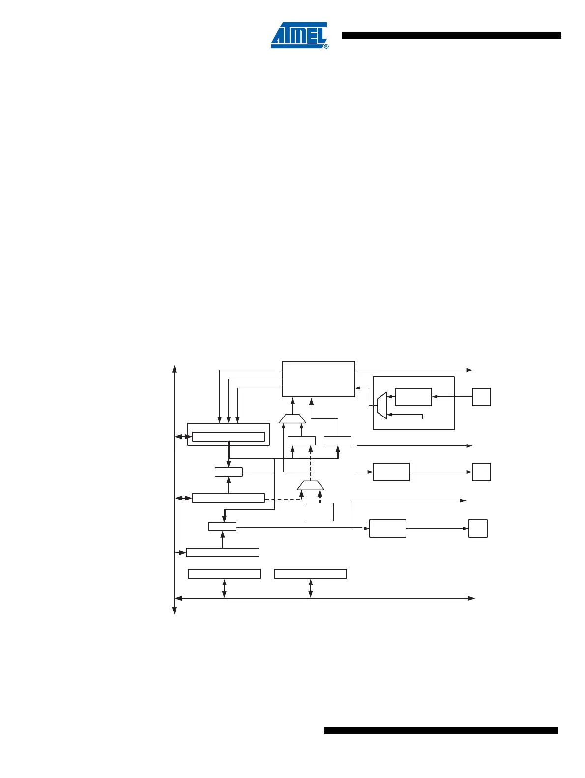
A simplified block diagram of the 8-bit Timer/Counter is shown in Figure 12-1. For the actual
placement of I/O pins, refer to “Pin Descriptions” on page 10. CPU accessible I/O Registers,
including I/O bits and I/O pins, are shown in bold. The device-specific I/O Register and bit loca-
tions are listed in the “8-bit Timer/Counter Register Description” on page 101.
The PRTIM0 bit in “Power Reduction Register” on page 42 must be written to zero to enable
Timer/Counter0 module.
Figure 12-1. 8-bit Timer/Counter Block Diagram
12.1.1 Definitions
Many register and bit references in this section are written in general form. A lower case “n”
replaces the Timer/Counter number, in this case 0. A lower case “x” replaces the Output Com-
pare Unit, in this case Compare Unit A or Compare Unit B. However, when using the register or
bit defines in a program, the precise form must be used, i.e., TCNT0 for accessing
Timer/Counter0 counter value and so on.
Timer/Counter
DATA BUS
=
TCNTn
Waveform
Generation
OCnA
Control Logic
count
clear
direction
TOVn
(Int.Req.)
OCRnx
TCCRnA
Clock Select
Tn
Edge
Detector
( From Prescaler )
clk
Tn
OCnA
(Int.Req.)
=
OCRnx
Waveform
Generation
OCnB
OCnB
(Int.Req.)
TCCRnB
=
Fixed
TOP
Values
=
0
TOP BOTTOM